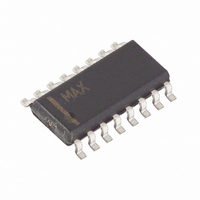
MAX4709ESE+ Maxim Integrated Products, MAX4709ESE+ Datasheet

MAX4709ESE+
Specifications of MAX4709ESE+
Related parts for MAX4709ESE+
MAX4709ESE+ Summary of contents
Page 1
... NO2 NO3 NO4 COM Pin Configurations/Functional Diagrams continued at end of data sheet. ________________________________________________________________ Maxim Integrated Products For pricing, delivery, and ordering information, please contact Maxim Direct at 1-888-629-4642, or visit Maxim’s website at www.maxim-ic.com. Fault-Protected, Single 8-to-1/ Dual 4-to-1 Multiplexers ♦ No Power-Supply Sequencing Required ♦ ...
Page 2
Fault-Protected, Single 8-to-1/ Dual 4-to-1 Multiplexers ABSOLUTE MAXIMUM RATINGS (All Voltages Referenced to GND) V+ ........................................................................-0.3V to +44.0V V- .........................................................................-44.0V to +0. V-................................................................-0.3V to +44.0V COM_, A_, EN (Note 1)........................ (V+ + 0.3V) to (V- - 0.3V) NO_.........................................................(V+ ...
Page 3
ELECTRICAL CHARACTERISTICS—Dual Supplies (continued) (V+ = +15V -15V +2.4V, V A_H T = +25°C.) (Note 2) A PARAMETER SYMBOL FAULT PROTECTION Fault-Protected Analog Signal Range (Notes 3, 4) COM_ Output Leakage Current, I Supplies On NO_ ...
Page 4
Fault-Protected, Single 8-to-1/ Dual 4-to-1 Multiplexers ELECTRICAL CHARACTERISTICS—Dual Supplies (continued) (V+ = +15V -15V +2.4V, V A_H T = +25°C.) (Note 2) A PARAMETER SYMBOL Channel-to-Channel Crosstalk NO_ Off-Capacitance C COM_ Off-Capacitance ...
Page 5
ELECTRICAL CHARACTERISTICS—Single +12V Supply (continued) (V+ = +12V +2.4V, V A_H A_L T = +25°C.) (Note 2) A PARAMETER SYMBOL COM_ On-Leakage Current I COM_(ON) FAULT PROTECTION Fault-Protected Analog Signal V NO Range (Notes 3, ...
Page 6
Fault-Protected, Single 8-to-1/ Dual 4-to-1 Multiplexers ELECTRICAL CHARACTERISTICS—Single +12V Supply (continued) (V+ = +12V +2.4V, V A_H A_L T = +25°C.) (Note 2) A PARAMETER SYMBOL Off-Isolation Channel-to-Channel Crosstalk POWER SUPPLY Power-Supply Range V+ Supply ...
Page 7
V- = -15V +2.4V ON-RESISTANCE vs. V AND TEMPERATURE COM (SINGLE SUPPLY) 1000 V+ = +12V T = +125° +70°C A 800 T = +85°C A ...
Page 8
Fault-Protected, Single 8-to-1/ Dual 4-to-1 Multiplexers (V+ = +15V -15V +2.4V FREQUENCY RESPONSE +15V V- = -15V 0 BANDWIDTH -20 -40 CROSSTALK OFF-ISOLATION -60 -80 -100 0.001 0.01 0.1 1 ...
Page 9
MAX4708 (Single 8-to-1 Mux) PIN NAME FUNCTION 1 A0 Address Bit Mux Enable Negative Supply Voltage. Bypass to GND 3 V- with a 0.1µF capacitor. 4 NO1 Channel Input 1 5 NO2 Channel Input 2 6 NO3 ...
Page 10
Fault-Protected, Single 8-to-1/ Dual 4-to-1 Multiplexers Detailed Description Several unique features differentiate the MAX4708/ MAX4709 from traditional fault-protected multiplexers. First, instead of the three series FETs utilized in older designs, the MAX4708/MAX4709 design employs two parallel FETs for lower on-resistance ...
Page 11
Applications Information V+ and GND power the internal logic and logic-level trans- lators. The logic-level translators convert the logic-level inputs to V+ and V- to drive the gates of the internal FETs. In this design, there is no galvanic connection ...
Page 12
Fault-Protected, Single 8-to-1/ Dual 4-to-1 Multiplexers V+ A2 NO1 A1 NO2–NO7 A0 MAX4708 NO8 +2.4V EN COM GND V- 50Ω V+ NO1B A1 A0 NO1A–NO4A NO4B MAX4709 +2.4V EN COMB GND V- 50Ω Figure 2. Address Transition Time V+ V ...
Page 13
+2.4V EN NO1–NO8 A0 MAX4708 COM GND V- 50Ω Figure 4. Break-Before-Make Interval MAX4708 CHANNEL A1 SELECT A2 GND Figure 5. Charge Injection ...
Page 14
Fault-Protected, Single 8-to-1/ Dual 4-to-1 Multiplexers V+ A2 NO1 CHANNEL A1 NO8 SELECT MAX4708 A0 COM GND EN V- Figure 8. NO_, COM_ Capacitance V+ MAX4708 NO1 NO2 NO3 NO4 NO5 NO6 NO7 NO8 DECODERS/DRIVERS MAX4709 NO1A ...
Page 15
... Maxim cannot assume responsibility for use of any circuitry other than circuitry entirely embodied in a Maxim product. No circuit patent licenses are implied. Maxim reserves the right to change the circuitry and specifications without notice at any time. Maxim Integrated Products, 120 San Gabriel Drive, Sunnyvale, CA 94086 408-737-7600 ____________________ 15 © 2008 Maxim Integrated Products ...


