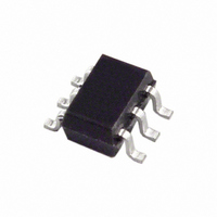
ADG749BKSZ-REEL7 Analog Devices Inc, ADG749BKSZ-REEL7 Datasheet - Page 4

ADG749BKSZ-REEL7
Manufacturer Part Number
ADG749BKSZ-REEL7
Description
IC SWITCH SPDT SC70-6
Manufacturer
Analog Devices Inc
Type
Analog Switchr
Datasheet
1.ADG749BKSZ-REEL.pdf
(12 pages)
Specifications of ADG749BKSZ-REEL7
Function
Switch
Circuit
1 x SPDT
On-state Resistance
5 Ohm
Voltage Supply Source
Single Supply
Voltage - Supply, Single/dual (±)
1.8 V ~ 5.5 V
Current - Supply
0.001µA
Operating Temperature
-40°C ~ 85°C
Mounting Type
Surface Mount
Package / Case
6-TSSOP, SC-88, SOT-363
Analog Switch Type
SPDT
No. Of Channels
1
Bandwidth
200MHz
On State Resistance Max
2.5ohm
Turn Off Time
3ns
Turn On Time
7ns
Supply Voltage Range
1.8V To 5.5V
Multiplexer Configuration
Single SPDT
Number Of Inputs
1
Number Of Outputs
2
Number Of Channels
1
Analog Switch On Resistance
12@3VOhm
Analog Switch Turn On Time
10ns
Analog Switch Turn Off Time
4ns
Package Type
SC-70
Power Supply Requirement
Single
Single Supply Voltage (min)
1.8V
Single Supply Voltage (typ)
3/5V
Single Supply Voltage (max)
5.5V
Dual Supply Voltage (min)
Not RequiredV
Dual Supply Voltage (typ)
Not RequiredV
Dual Supply Voltage (max)
Not RequiredV
Power Dissipation
315mW
Supply Current
0.001mA
Mounting
Surface Mount
Pin Count
6
Operating Temp Range
-40C to 125C
Operating Temperature Classification
Automotive
Lead Free Status / RoHS Status
Lead free / RoHS Compliant
Lead Free Status / RoHS Status
Lead free / RoHS Compliant, Lead free / RoHS Compliant
Other names
ADG749BKSZ-REEL7TR
Available stocks
Company
Part Number
Manufacturer
Quantity
Price
Company:
Part Number:
ADG749BKSZ-REEL7
Manufacturer:
AD
Quantity:
500
Company:
Part Number:
ADG749BKSZ-REEL7
Manufacturer:
NSC
Quantity:
147
Part Number:
ADG749BKSZ-REEL7
Manufacturer:
ADI/亚德诺
Quantity:
20 000
ADG749
V
Table 2.
Parameter
ANALOG SWITCH
LEAKAGE CURRENTS
DIGITAL INPUTS
DYNAMIC CHARACTERISTICS
t
POWER REQUIREMENTS
1
D
Guaranteed by design, not subject to production test.
Analog Signal Range
On Resistance (R
On Resistance Match Between
Channels (ΔR
On Resistance Flatness (R
Source Off Leakage IS (Off )
Channel On Leakage I
Input High Voltage, V
Input Low Voltage, V
Input Current
I
t
t
Break-Before-Make Time Delay,
Off Isolation
Channel-to-Channel Crosstalk
Bandwidth −3 dB
C
C
I
DD
INL
DD
ON
OFF
S
D
, C
(Off )
or I
= 3 V ± 10% and GND = 0 V; T
S
(On)
INH
ON
)
ON
)
1
INL
INH
D
, I
S
FLAT(ON)
(On)
1
)
25°C
6
±0.01
±0.25
±0.01
±0.25
0.005
10
4
8
–67
–87
–82
7
27
0.001
A
–62
200
= −40°C to +125°C unless otherwise stated
7
2.5
±0.35
±0.35
2.0
0.8
−40°C to +85°C
10
0.1
0.8
Rev. B | Page 4 of 12
−40°C to +125°C
0 V to V
12
0.8
1
5
±0.1
15
8
1
1.0
DD
Unit
V
Ω typ
Ω max
Ω typ
Ω max
Ω typ
nA typ
nA max
nA typ
nA max
V min
V max
μA typ
μA max
ns typ
ns max
ns typ
ns max
ns typ
ns min
dB typ
dB typ
dB typ
dB typ
MHz typ
pF typ
pF typ
μA typ
μA max
Test Conditions/Comments
V
see Figure 13
V
V
V
V
see Figure 14
V
see Figure 15
V
R
V
R
V
R
V
R
R
R
R
R
V
Digital inputs = 0 V or 3.3 V
S
S
S
DD
S
S
IN
L
S
L
S
L
S1
L
L
L
L
L
DD
= 0 V to V
= 0 V to V
= 0 V to V
= 3 V/1 V, V
= V
= 300 Ω, C
= 2 V; see Figure 16
= 300 Ω, C
= 2 V; see Figure 16
= 300 Ω, C
= 50 Ω, C
= 50 Ω, C
= 50 Ω, C
= 50 Ω, C
= 50 Ω, C
= V
= V
= 3.3 V
= 3.3 V
D
INL
S2
= 1 V or V
= 2 V; see Figure 17
or V
L
L
L
L
L
DD
DD
DD
INH
= 5 pF, f = 10 MHz
= 5 pF, f = 1 MHz; see Figure 18
= 5 pF, f = 10 MHz
= 5 pF, f = 1 MHz; see Figure 19
= 5 pF; see Figure 20
L
L
L
D
, I
, I
, I
= 35 pF
= 35 pF
= 35 pF
= 1 V/3 V;
S
S
S
= –10 mA;
= –10 mA
= –10 mA
S
= V
D
= 3 V;


