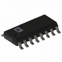
ADG713BR-REEL Analog Devices Inc, ADG713BR-REEL Datasheet - Page 2

ADG713BR-REEL
Manufacturer Part Number
ADG713BR-REEL
Description
IC SWITCH QUAD SPST 16SOIC
Manufacturer
Analog Devices Inc
Datasheet
1.ADG711BRUZ.pdf
(12 pages)
Specifications of ADG713BR-REEL
Rohs Status
RoHS non-compliant
Function
Switch
Circuit
4 x SPST - NC/NO
On-state Resistance
4 Ohm
Voltage Supply Source
Single Supply
Voltage - Supply, Single/dual (±)
1.8 V ~ 5.5 V
Current - Supply
0.001µA
Operating Temperature
-40°C ~ 85°C
Mounting Type
Surface Mount
Package / Case
16-SOIC (0.154", 3.90mm Width)
Available stocks
Company
Part Number
Manufacturer
Quantity
Price
Company:
Part Number:
ADG713BR-REEL7
Manufacturer:
SEMTECH
Quantity:
1 758
ADG711/ADG712/ADG713–SPECIFICATIONS
Parameter
LEAKAGE CURRENTS
DIGITAL INPUTS
DYNAMIC CHARACTERISTICS
POWER REQUIREMENTS
NOTES
1
2
Specifications subject to change without notice.
ANALOG SWITCH
Temperature range: B Version: –40°C to +85°C.
Guaranteed by design, not subject to production test.
On Resistance (R
On Resistance Match Between
On Resistance Flatness (R
Source OFF Leakage I
Drain OFF Leakage I
Channel ON Leakage I
Input High Voltage, V
Input Low Voltage, V
Input Current
t
t
Break-Before-Make Time Delay, t
Charge Injection
Off Isolation
Channel-to-Channel Crosstalk
Bandwidth –3 dB
C
C
C
I
Analog Signal Range
OFF
ON
DD
S
D
D
I
Channels (∆R
(ADG713 Only)
INL
(OFF)
, C
(OFF)
S
or I
(ON)
INH
ON
ON
)
)
D
INL
INH
S
D
(OFF)
(OFF)
, I
FLAT(ON)
S
(ON)
2
D
)
2.5
4
0.5
± 0.01
± 0.1
± 0.01
± 0.1
± 0.01
± 0.1
0.005
11
6
6
3
–58
–78
–90
200
10
10
22
0.001
+25 C
B Version
–40 C to
+85 C
0 V to V
4.5
0.05
0.3
1.0
± 0.2
± 0.2
± 0.2
2.4
0.8
± 0.1
16
10
1
1.0
–2–
DD
Unit
V
Ω typ
Ω max
Ω typ
Ω max
Ω typ
Ω max
nA typ
nA max
nA typ
nA max
nA typ
nA max
V min
V max
µA typ
µA max
ns typ
ns max
ns typ
ns max
ns typ
ns min
pC typ
dB typ
dB typ
dB typ
MHz typ
pF typ
pF typ
pF typ
µA typ
µA max
1
(V
–40 C to +85 C unless otherwise noted.)
DD
= +5 V
Test Conditions/Comments
V
Test Circuit 1
V
V
V
V
Test Circuit 2
V
Test Circuit 2
V
Test Circuit 3
V
R
V
R
V
R
V
V
Test Circuit 6
R
R
Test Circuit 7
R
Test Circuit 8
R
V
Digital Inputs = 0 V or 5 V
S
S
S
DD
S
S
S
IN
S
S
S1
S
L
DD
L
L
L
L
L
L
= 0 V to V
= 0 V to V
= 0 V to V
= 4.5 V/1 V, V
= 4.5 V/1 V, V
= V
= 3 V; Test Circuit 4
= 3 V; Test Circuit 4
= 2 V; R
= 50 Ω, C
= 300 Ω, C
= 300 Ω, C
= 300 Ω, C
= 50 Ω, C
= 50 Ω, C
= 50 Ω, C
= V
= V
= +5.5 V;
= +5.5 V
D
S2
INL
10%, GND = 0 V. All specifications
= 1 V, or 4.5 V;
= 3 V; Test Circuit 5
or V
S
L
= 0 Ω, C
L
L
L
DD
DD
DD
= 5 pF, f = 10 MHz
L
L
L
= 5 pF, f = 1 MHz;
= 5 pF, f = 10 MHz;
= 5 pF; Test Circuit 9
INH
, I
, I
, I
= 35 pF,
= 35 pF,
= 35 pF,
D
D
S
S
S
= 1 V/4.5 V;
= 1 V/4.5 V;
= –10 mA;
= –10 mA
= –10 mA
L
= 1 nF;
REV. A


