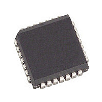
CY7B933-JCT Cypress Semiconductor Corp, CY7B933-JCT Datasheet - Page 4

CY7B933-JCT
Manufacturer Part Number
CY7B933-JCT
Description
Manufacturer
Cypress Semiconductor Corp
Datasheet
1.CY7B933-JCT.pdf
(33 pages)
Specifications of CY7B933-JCT
Lead Free Status / Rohs Status
Not Compliant
Available stocks
Company
Part Number
Manufacturer
Quantity
Price
Company:
Part Number:
CY7B933-JCT
Manufacturer:
NVIDIA
Quantity:
6 000
Document #: 38-02017 Rev. *E
CY7B923 HOTLink Transmitter (continued)
CY7B933 HOTLink Receiver
V
V
GND
Q
(Q
SC/D (Q
RVS (Q
RDY
CKR
A/B
INA±
INB
(INB+)
SI
(INB−)
SO
RF
Name
Name
CCN
CCQ
0−7
b − h
)
j
a
)
)
TTL Out
TTL Out
TTL Out
TTL Out
TTL Out
PECL in
Diff In
PECL in
(Diff In)
PECL in
(Diff In)
TTL Out
TTL In
I/O
I/O
Power for output drivers.
Power for internal circuitry.
Ground.
Q
synchronously with CKR. When MODE is HIGH, Q
Special Character/Data Select. SC/D indicates the context of received data. HIGH indicates a
Control (Special Character) code, LOW indicates a Data character. When MODE is HIGH (placing the
receiver in Unencoded mode), SC/D acts as the Q
Received Violation Symbol. A HIGH on RVS indicates that a code rule violation has been detected
in the received data stream. A LOW shows that no error has been detected. In BIST mode, a LOW
on RVS indicates correct operation of the Transmitter, Receiver, and link on a byte-by-byte basis.
When MODE is HIGH (placing the receiver in Unencoded mode), RVS acts as the Q
the same timing as Q
Data Output Ready. A LOW pulse on RDY indicates that new data has been received and is ready
to be delivered. A missing pulse on RDY shows that the received data is the Null character (normally
inserted by the transmitter as a pad between data inputs). In BIST mode RDY will remain LOW for all
but the last byte of a test loop and will pulse HIGH one byte time per BIST loop.
Clock Read. This byte rate clock output is phase and frequency aligned to the incoming serial data
stream. RDY, Q
Serial Data Input Select. This PECL 100K (+5V referenced) input selects INA or INB as the active
data input. If A/B is HIGH, INA is connected to the shifter and signals connected to INA will be decoded.
If A/B is LOW INB is selected.
Serial Data Input A. The differential signal at the receiver end of the communication link may be
connected to the differential input pairs INA± or INB±. Either the INA pair or the INB pair can be used
as the main data input and the other can be used as a loopback channel or as an alternative data
input selected by the state of A/B. One input of an intentionally unused differential-pair (INA± or INB±)
should be terminated to V
tally created.
Serial Data Input B. This pin is either a single-ended PECL data receiver (INB) or half of the INB
differential pair. If SO is wired to V
changeably with INA±. If SO is normally connected and loaded, INB becomes a single-ended PECL
100K (+5V referenced) serial data input. INB is used as the test clock while in Test mode.
Status Input. This pin is either a single-ended PECL status monitor input (SI) or half of the INB
differential pair. If SO is wired to V
changeably with INA±. If SO is normally connected and loaded, SI becomes a single-ended PECL
100K (+5V referenced) status monitor input, which is translated into a TTL-level signal at the SO pin.
Status Out. SO is the TTL-translated output of SI. It is typically used to translate the Carrier Detect
output from a fiber-optic receiver connected to SI. When this pin is normally connected and loaded
(without any external pull-up resistor), SO will assume the same logical level as SI and INB will become
a single-ended PECL serial data input. If the status monitor translation is not desired, then SO may
be wired to V
Reframe Enable. RF controls the Framer logic in the Receiver. When RF is held HIGH, each SYNC
(K28.5) symbol detected in the shifter will frame the data that follows. If it is HIGH for 2,048 consecutive
bytes, the internal framer switches to double-byte mode. When RF is held LOW, the reframing logic
is disabled. The incoming data stream is then continuously deserialized and decoded using byte
boundaries set by the internal byte counter. Bit errors in the data stream will not cause alias SYNC
characters to reframe the data erroneously.
Description
Description
0–7
Parallel Data Output. Q
CC
0−7
and the INB± pair may be used as a differential serial data input.
, SC/D, and RVS all switch synchronously with the rising edge of this output.
0−7
.
CC
through a 1−5 KΩ resistor to assure that no data transitions are acciden-
0–7
contain the most recently received data. These outputs change
CC
CC
, then INB± can be used as differential line receiver inter-
, then INB± can be used as differential line receiver inter-
a
0, 1, ...7
output. SC/D has the same timing as Q
become Q
b, c,...h
, respectively.
j
CY7B923
CY7B933
output. RVS has
Page 4 of 33
0−7
.
[+] Feedback


