HI1-0303-2 Intersil, HI1-0303-2 Datasheet - Page 3
HI1-0303-2
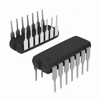
Manufacturer Part Number
HI1-0303-2
Description
IC SWITCH DUAL SPDT 14CDIP
Manufacturer
Intersil
Datasheet
1.HI1-0303R5254.pdf
(11 pages)
Specifications of HI1-0303-2
Function
Switch
Circuit
2 x SPDT
On-state Resistance
50 Ohm
Voltage Supply Source
Single, Dual Supply
Voltage - Supply, Single/dual (±)
5 V ~ 34 V, ±5 V ~ 20 V
Operating Temperature
-55°C ~ 125°C
Mounting Type
Through Hole
Package / Case
14-CDIP (0.300", 7.62mm)
Lead Free Status / RoHS Status
Contains lead / RoHS non-compliant


Absolute Maximum Ratings
Voltage Between Supplies (V+ to V-) . . . . . . . . . . . . . . . . 44V (±22V)
Digital Input Voltage . . . . . . . . . . . . . . . . . . . . . . (V+) +4V to (V-) -4V
Analog Input Voltage . . . . . . . . . . . . . . . . . . (V+) +1.5V to (V-) -1.5V
Typical Derating Factor . . . . . . . . . 1.5mA/MHz Increase in ICCOP
ESD Classification . . . . . . . . . . . . . . . . . . . . . . . . . . . . . . . . . Class 1
Operating Conditions
Temperature Range
CAUTION: Stresses above those listed in “Absolute Maximum Ratings” may cause permanent damage to the device. This is a stress only rating and operation of the
device at these or any other conditions above those indicated in the operational sections of this specification is not implied.
NOTE:
Electrical Specifications
DYNAMIC CHARACTERISTICS
Switch ON Time, t
Switch OFF Time, t
Break-Before-Make Delay, t
Charge Injection Voltage, ∆V (Note 7)
OFF Isolation (Note 6)
Input Switch Capacitance, C
Output Switch Capacitance, C
Output Switch Capacitance, C
Digital Input Capacitance, C
DIGITAL INPUT CHARACTERISTICS
Input Low Level, V
Input High Level, V
Input Leakage Current (Low), I
Input Leakage Current (High), I
ANALOG SWITCH CHARACTERISTICS
Analog Signal Range
ON Resistance, r
OFF Input Leakage Current, I
OFF Output Leakage Current, I
ON Leakage Current, I
1. θ
HI-303-2 . . . . . . . . . . . . . . . . . . . . . . . . . . . . . . . . -55
HI-303-5 . . . . . . . . . . . . . . . . . . . . . . . . . . . . . . . . . . 0
HI-303-9 . . . . . . . . . . . . . . . . . . . . . . . . . . . . . . . . . -40
JA
is measured with the component mounted on a low effective thermal conductivity test board in free air. See Tech Brief TB379 for details.
ON
ON
PARAMETER
INL
INH
OFF
(Note 2)
D(ON)
(Note 10)
OPEN
IN
S(OFF)
(Note 4)
S(OFF)
D(OFF)
D(ON)
INL
INH
D(OFF)
3
(Note 5)
Supplies = +15V, -15V; V
Unless Otherwise Specified
(Note 5)
(Note 3)
(Note 3)
o
C to 125
o
o
C to 75
C to 85
TEMP
(
Full
Full
Full
Full
Full
Full
Full
Full
Full
IN
o
25
25
25
25
25
25
25
25
25
25
25
25
25
C)
= Logic Input. V
o
o
o
C
C
C
HI-303
MIN
-15
4
-
-
-
-
-
-
-
-
-
-
-
-
-
-
-
-
-
-
-
-
Thermal Information
Thermal Resistance (Typical, Note 1)
Maximum Junction Temperature
Maximum Storage Temperature Range . . . . . . . . . . -65
Maximum Lead Temperature (Soldering 10s) . . . . . . . . . . . . 300
IN
CERDIP Package. . . . . . . . . . . . . . . . .
PDIP Package . . . . . . . . . . . . . . . . . . .
SOIC Package . . . . . . . . . . . . . . . . . . .
Ceramic Packages . . . . . . . . . . . . . . . . . . . . . . . . . . . . . . . 175
Plastic Packages . . . . . . . . . . . . . . . . . . . . . . . . . . . . . . . . 150
(SOIC - Lead Tips Only)
- for Logic “1” = 4V, for Logic “0” = 0.8V.
TYP
0.04
0.04
0.03
210
160
0.5
60
60
16
14
35
35
40
-2
3
5
1
1
-
-
-
-
-
MAX
300
250
+15
100
100
100
0.8
50
75
1
1
1
1
1
-
-
-
-
-
-
-
-
MIN
-15
4
-
-
-
-
-
-
-
-
-
-
-
-
-
-
-
-
-
-
-
-
-5, -9
TYP
0.04
0.04
0.03
210
160
0.2
0.2
0.2
60
60
16
14
35
35
40
3
5
-
-
-
-
-
θ
JA
120
(
80
90
o
C/W) θ
MAX
300
250
+15
100
100
100
0.8
50
75
1
1
5
5
5
-
-
-
-
-
-
-
-
November 17, 2004
o
C to 150
JC
UNITS
FN3125.10
N/A
N/A
(
24
mV
dB
pF
pF
pF
pF
µA
µA
nA
nA
nA
nA
nA
nA
o
ns
ns
ns
Ω
Ω
V
V
V
C/W)
o
o
o
o
C
C
C
C
Related parts for HI1-0303-2
Image
Part Number
Description
Manufacturer
Datasheet
Request
R

Part Number:
Description:
HI1-303-5IC,ANALOG SWITCH,DUAL,SPDT,CMOS,DIP,14PIN
Manufacturer:
Intersil Corporation
Datasheet:
Part Number:
Description:
300 MIL PDIP/CDIP//MUX DIFF 4:1 OVP 16CDIP /883
Manufacturer:
Intersil Corporation
Part Number:
Description:
DAC 12BIT 6.7MHZ 0.25LSB 24 S/B DIP /883
Manufacturer:
Intersil Corporation
Datasheet:

Part Number:
Description:
IC ADC 12BIT 40KSPS 1CH 28-SBDIP
Manufacturer:
Intersil
Datasheet:
Part Number:
Description:
IC ADC 12BIT 40KSPS 1CH 28-SBDIP
Manufacturer:
Intersil
Datasheet:
Part Number:
Description:
IC ADC 12BIT 67KSPS 1CH 28-SBDIP
Manufacturer:
Intersil
Datasheet:
Part Number:
Description:
IC ADC 12BIT 40KSPS 1CH 28-SBDIP
Manufacturer:
Intersil
Datasheet:
Part Number:
Description:
IC ADC 12BIT 40KSPS 1CH 28-SBDIP
Manufacturer:
Intersil
Datasheet:

Part Number:
Description:
CONV D/A 12BIT 6.7MHZ 24-DIP
Manufacturer:
Intersil
Datasheet:
Part Number:
Description:
CONV D/A 12BIT 6.7MHZ 24-DIP
Manufacturer:
Intersil
Datasheet:

Part Number:
Description:
IC SWITCH QUAD SPST 16CDIP
Manufacturer:
Intersil
Datasheet:
Part Number:
Description:
IC MULTIPLEXER 8X1 16CDIP
Manufacturer:
Intersil
Datasheet:
Part Number:
Description:
IC SWITCH QUAD SPST 16CDIP
Manufacturer:
Intersil
Datasheet: