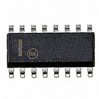
MC74VHC4051DR2G ON Semiconductor, MC74VHC4051DR2G Datasheet - Page 4

MC74VHC4051DR2G
Manufacturer Part Number
MC74VHC4051DR2G
Description
IC MUX/DEMUX 8X1 16SOIC
Manufacturer
ON Semiconductor
Series
74VHCr
Datasheet
1.MC74VHC4052DR2G.pdf
(16 pages)
Specifications of MC74VHC4051DR2G
Function
Multiplexer/Demultiplexer
Circuit
1 x 8:1
On-state Resistance
125 Ohm
Voltage Supply Source
Dual Supply
Voltage - Supply, Single/dual (±)
±2 V ~ 6 V, 2 V ~ 12 V
Current - Supply
40µA
Operating Temperature
-55°C ~ 125°C
Mounting Type
Surface Mount
Package / Case
16-SOIC (0.154", 3.90mm Width)
On Resistance (max)
200 Ohms
Propagation Delay Time
40 ns
On Time (max)
245 ns
Off Time (max)
160 ns
Supply Voltage (max)
6 V
Supply Voltage (min)
2 V
Maximum Power Dissipation
500 mW
Maximum Operating Temperature
+ 125 C
Minimum Operating Temperature
- 55 C
Mounting Style
SMD/SMT
Number Of Switches
Single
Lead Free Status / RoHS Status
Lead free / RoHS Compliant
Available stocks
Company
Part Number
Manufacturer
Quantity
Price
Company:
Part Number:
MC74VHC4051DR2G
Manufacturer:
ON
Quantity:
2 500
Company:
Part Number:
MC74VHC4051DR2G
Manufacturer:
ON Semiconductor
Quantity:
3 400
Part Number:
MC74VHC4051DR2G
Manufacturer:
ON/安森美
Quantity:
20 000
*Maximum Ratings are those values beyond which damage to the device may occur.
†Derating — SOIC Package: – 7 mW/_C from 65_ to 125_C
*For voltage drops across switch greater than 1.2V (switch on), excessive V
MAXIMUM RATINGS*
RECOMMENDED OPERATING CONDITIONS
Symbol
Functional operation should be restricted to the Recommended Operating Conditions.
drawn; i.e., the current out of the switch may contain both V
The reliability of the device will be unaffected unless the Maximum Ratings are exceeded.
Symbol
V
V
T
V
V
P
V
V
V
T
t
V
V
CC
stg
EE
T
r
I
IS
in
D
IO
, t
L
CC
EE
IS
in
A
f
*
Positive DC Supply Voltage
Negative DC Supply Voltage (Referenced to GND)
Analog Input Voltage
Digital Input Voltage (Referenced to GND)
DC Current, Into or Out of Any Pin
Power Dissipation in Still Air
Storage Temperature Range
Lead Temperature, 1 mm from Case for 10 Seconds
Positive DC Supply Voltage
Negative DC Supply Voltage, Output (Referenced to GND)
Analog Input Voltage
Digital Input Voltage (Referenced to GND)
Static or Dynamic Voltage Across Switch
Operating Temperature Range, All Package Types
Input Rise/Fall Time
TSSOP Package: -- 6.1 mW/_C from 65_ to 125_C
(Channel Select or Enable Inputs)
Parameter
(Referenced to GND)
(Referenced to V
TSSOP Package†
SOIC Package†
(Referenced to GND)
(Referenced to V
Parameter
http://onsemi.com
V
V
V
V
CC
CC
CC
CC
CC
EE
and switch input components.
= 3.0 V
)
= 2.0 V
= 4.5 V
= 6.0 V
– 0.5 to V
EE
4
– 0.5 to + 14.0
– 0.5 to + 7.0
– 7.0 to + 5.0
– 65 to + 150
V
)
V
EE
CC
Value
CC
± 25
500
450
260
-- 0.5 to
+ 0.5
CC
current may be
+ 0.5
Unit
mW
mA
_C
_C
V
V
V
V
circuitry to guard against damage
due to high static voltages or electric
fields. However, precautions must
be taken to avoid applications of any
voltage higher than maximum rated
voltages to this high--impedance cir-
cuit. For proper operation, V
V
range GND ≤ (V
tied to an appropriate logic voltage
level (e.g., either GND or V
Unused outputs must be left open.
out
This device contains protection
Unused inputs must always be
should be constrained to the
GND
-- 6.0
– 55
Min
V
2.0
2.0
in
0
0
0
0
EE
or V
+ 125
out
GND
1000
Max
12.0
V
V
800
500
400
6.0
1.2
CC
CC
) ≤ V
in
CC
CC
Unit
and
_C
ns
V
V
V
V
V
).
.


