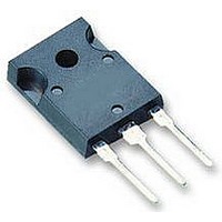
AUIRFP064N International Rectifier, AUIRFP064N Datasheet - Page 2

AUIRFP064N
Manufacturer Part Number
AUIRFP064N
Description
54T8873
Manufacturer
International Rectifier
Datasheet
1.AUIRFP064N.pdf
(11 pages)
Specifications of AUIRFP064N
Transistor Polarity
N Channel
Continuous Drain Current Id
110A
Drain Source Voltage Vds
55V
On Resistance Rds(on)
0.008ohm
Rds(on) Test Voltage Vgs
10V
Power Dissipation Pd
200W
Rohs Compliant
Yes
Drain-source Breakdown Voltage
55 V
Gate-source Breakdown Voltage
20 V
Continuous Drain Current
110 A
Power Dissipation
200 W
Mounting Style
Through Hole
Package / Case
TO-247AC
Gate Charge Qg
113.3 nC
Lead Free Status / Rohs Status
Details
Available stocks
Company
Part Number
Manufacturer
Quantity
Price
Company:
Part Number:
AUIRFP064N
Manufacturer:
IR
Quantity:
12 500
‚
ƒ
Notes:
Static Electrical Characteristics @ T
V
ΔV
R
V
gfs
I
I
Dynamic Electrical Characteristics @ T
Q
Q
Q
t
t
t
t
L
L
C
C
C
Diode Characteristics
I
I
V
t
Q
DSS
GSS
d(on)
r
d(off)
f
S
SM
rr
D
S
Repetitive rating; pulse width limited by
max. junction temperature. (See fig. 11).
V
R
I
(BR)DSS
GS(th)
SD
DS(on)
iss
oss
rss
g
gs
gd
rr
SD
2
DD
(BR)DSS
G
= 25Ω, I
≤
= 25V, starting T
/ΔT
AS
J
= 59A.(See Figure 12)
Drain-to-Source Breakdown Voltage
Breakdown Voltage Temp. Coefficient
Static Drain-to-Source On-Resistance
Gate Threshold Voltage
Forward Transconductance
Drain-to-Source Leakage Current
Gate-to-Source Forward Leakage
Gate-to-Source Reverse Leakage
Total Gate Charge
Gate-to-Source Charge
Gate-to-Drain ("Miller") Charge
Turn-On Delay Time
Rise Time
Turn-Off Delay Time
Fall Time
Internal Drain Inductance
Internal Source Inductance
Input Capacitance
Output Capacitance
Reverse Transfer Capacitance
Continuous Source Current
(Body Diode)
Pulsed Source Current
(Body Diode)
Diode Forward Voltage
Reverse Recovery Time
Reverse Recovery Charge
≤
J
= 25°C, L = 190μH,
Parameter
DD
Parameter
≤
™
(BR)DSS
J
≤
J
= 25°C (unless otherwise specified)
J
= 25°C (unless otherwise specified)
Min. Typ. Max. Units
Min. Typ. Max. Units
–––
–––
–––
–––
–––
–––
–––
–––
–––
–––
–––
–––
–––
–––
–––
–––
–––
–––
–––
–––
–––
–––
–––
2.0
55
42
„
…
Pulse width ≤ 300
Calculated continuous current based on maximum allowable
junction temperature; for recommended current-handling of the
package refere to Desing Tip # 93-4
0.057
4000
1300
–––
–––
–––
–––
–––
–––
–––
–––
–––
–––
–––
100
480
–––
–––
–––
110
450
5.0
14
43
70
13
0.008
110
-100
–––
–––
–––
–––
170
680
250
100
170
–––
–––
–––
–––
–––
–––
–––
–––
390
4.0
1.3
25
32
74
g
V/°C
; duty cycle ≤ 2%
μA
nA
nC
nH
pF
nC
ns
ns
V
Ω
V
S
A
V
V
Reference to 25°C, I
V
V
V
V
V
V
V
I
V
V
V
I
R
R
Between lead,
6mm (0.25in.)
from package
and center of die contact
V
V
ƒ = 1.0MHz,See Fig.5
MOSFET symbol
showing the
integral reverse
p-n junction diode.
T
T
di/dt = 100A/μs
D
D
J
J
GS
GS
DS
DS
DS
DS
GS
GS
DS
GS
DD
G
D
GS
DS
= 59A
= 59A
= 25°C, I
= 25°C, I
= 0.39Ω,See Fig.10
= 2.5Ω
= V
= 25V, I
= 55V, V
= 44V, V
= 44V
= 25V
= 0V, I
= 10V, I
= 20V
= -20V
= 10V,See Fig.6 and 13
= 28V
= 0V
GS
, I
D
D
S
F
Conditions
Conditions
D
D
= 250μA
GS
GS
= 59A, V
= 59A
= 250μA
= 59A
= 59A
= 0V
= 0V, T
f
f
D
f
GS
= 1mA
J
f
www.irf.com
= 150°C
= 0V
G
f
f
S
D


