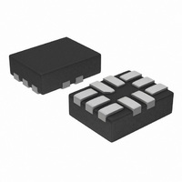
NLAS7222AMUTAG ON Semiconductor, NLAS7222AMUTAG Datasheet

NLAS7222AMUTAG
Specifications of NLAS7222AMUTAG
Available stocks
Related parts for NLAS7222AMUTAG
NLAS7222AMUTAG Summary of contents
Page 1
... NLAS7222A High-Speed USB 2.0 (480 Mbps) DPDT Switch ON Semiconductor's NLAS7222A series of analog switch circuits are produced using the company's advanced sub-micron CMOS technology, achieving industry-leading performance. The NLAS7222A 1-port analog switch. Its wide bandwidth and low bit-to-bit skew allow it to pass high-speed differential signals with good signal integrity ...
Page 2
HSD1- HSD2 CONTROL HSD1+ HSD2+ Figure 1. Pin Connections and Logic Diagram (Top View) MAXIMUM RATINGS Symbol V Positive DC Supply Voltage CC V Analog Switch Input Voltage IS ...
Page 3
DC ELECTRICAL CHARACTERISTICS FOR USB 2.0 SWITCHING OVER OPERATIONAL RANGE Symbol Parameter V Input HIGH Voltage ( Input LOW Voltage ( Clamp Diode Voltage IK I Quiescent Supply Current CC I Increase ...
Page 4
DUT V Output CC 0 Switch Select Pin DUT V Output CC 0.1 mF Open Input DUT Output Open Input NLAS7222A V CC Input GND V OUT 35 pF Output Figure 2. t (Time Break-Before-Make) BBM V ...
Page 5
W Generator Channel switch control/s test socket is normalized. Off isolation is measured across an off channel. On loss is the bandwidth switch Off Channel Isolation = 20 Log ISO ...
Page 6
The low on resistance and capacitance of the NLAS7222A provides for a high bandwidth analog switch suitable for applications such as USB data switching. Results for the USB 2.0 signal quality tests will be shown in this section, along with ...
Page 7
NLAS7222A Figure 8. Block Diagram of the NLAS7222A USB Demo Board Figure 9. Photograph of the NLAS7222A USB Demo Board http://onsemi.com 7 ...
Page 8
AND8267/D – NLAS7222A USB 2.0 Signal Quality Compliance Tests Figures 10, 11 and 12 show the test results for USB eye diagram tests. A summary of the USB tests is provided in Table 3. The NLAS7222A passes the low, full ...
Page 9
... Paired KJ Jitter Range -1.9 to 1.1 ns, RMS jitter = 1.0 ns ORDERING INFORMATION Device NLAS7222AMTR2G NLAS7222AMUR2G NLAS7222AMUTAG †For information on tape and reel specifications, including part orientation and tape sizes, please refer to our Tape and Reel Packaging Specifications Brochure, BRD8011/D. NLAS7222A Low Speed Full Speed Pass Pass 166 ...
Page 10
D A É É É É E É É PIN 1 REFERENCE 0. 0. 0. ...
Page 11
... Opportunity/Affirmative Action Employer. This literature is subject to all applicable copyright laws and is not for resale in any manner. PUBLICATION ORDERING INFORMATION LITERATURE FULFILLMENT: Literature Distribution Center for ON Semiconductor P.O. Box 5163, Denver, Colorado 80217 USA Phone: 303-675-2175 or 800-344-3860 Toll Free USA/Canada Fax: 303-675-2176 or 800-344-3867 Toll Free USA/Canada ...


