MC14553BCP ON Semiconductor, MC14553BCP Datasheet
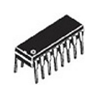
MC14553BCP

Manufacturer Part Number
MC14553BCP
Description
Manufacturer
ON Semiconductor
Type
Decader
Datasheet

Specifications of MC14553BCP

Technology
CMOS
Number Of Elements
3
Number Of Bits
3
Logic Family
4000
Logical Function
Counter
Operating Supply Voltage (typ)
3.3/5/9/12/15V
Output Type
Standard
Package Type
PDIP
Propagation Delay Time
1800ns
Operating Temp Range
-55C to 125C
Operating Supply Voltage (min)
3V
Operating Supply Voltage (max)
18V
Operating Temperature Classification
Military
Mounting
Through Hole
Pin Count
16
Lead Free Status / Rohs Status
Not Compliant

Available stocks

Company
Part Number
Manufacturer
Quantity
Price
Part Number:
MC14553BCP
Manufacturer:
MOT
Quantity:
5 510
Part Number:
MC14553BCP
Manufacturer:
ON
Quantity:
6
Part Number:
MC14553BCP
Manufacturer:
ON/安森美
Quantity:
20 000
Part Number:
MC14553BCPG
Manufacturer:
SILICON
Quantity:
254
Part Number:
MC14553BCPG
Manufacturer:
ON/安森美
Quantity:
20 000
MC14553B
3−Digit BCD Counter
triggered BCD counters that are cascaded synchronously. A quad latch
at the output of each counter permits storage of any given count. The
information is then time division multiplexed, providing one BCD
number or digit at a time. Digit select outputs provide display control.
All outputs are TTL compatible.
which drives the multiplexer output selector.
digital panel meters, and as a building block for general logic
applications.
Features
Stresses exceeding Maximum Ratings may damage the device. Maximum
Ratings are stress ratings only. Functional operation above the Recommended
Operating Conditions is not implied. Extended exposure to stresses above the
Recommended Operating Conditions may affect device reliability.
1. Temperature Derating: Plastic “P and D/DW”
static voltages or electric fields. However, precautions must be taken to avoid
applications of any voltage higher than maximum rated voltages to this
high−impedance circuit. For proper operation, V
the range V
(e.g., either V
*For additional information on our Pb−Free strategy and soldering details, please
MAXIMUM RATINGS
© Semiconductor Components Industries, LLC, 2006
June, 2006 − Rev. 7
download the ON Semiconductor Soldering and Mounting Techniques
Reference Manual, SOLDERRM/D.
DC Supply Voltage Range
Input or Output Voltage Range
(DC or Transient)
Input Current (DC or Transient) per Pin
Output Current (DC or Transient) per Pin
Power Dissipation, per Package (Note 1)
Ambient Temperature Range
Storage Temperature Range
Lead Temperature (8−Second Soldering)
The MC14553B 3−digit BCD counter consists of 3 negative edge
An on−chip oscillator provides the low−frequency scanning clock
This device is used in instrumentation counters, clock displays,
This device contains protection circuitry to guard against damage due to high
Unused inputs must always be tied to an appropriate logic voltage level
TTL Compatible Outputs
On−Chip Oscillator
Cascadable
Clock Disable Input
Pulse Shaping Permits Very Slow Rise Times on Input Clock
Output Latches
Master Reset
Pb−Free Packages are Available*
Packages: – 7.0 mW/_C From 65_C To 125_C
SS
SS
v (V
or V
Parameter
in
DD
or V
). Unused outputs must be left open.
(Voltages Referenced to V
out
) v V
DD
.
in
Symbol
and V
V
V
V
T
I
P
T
T
I
out
DD
out
stg
in
in
D
A
L
,
SS
out
)
should be constrained to
−0.5 to +18.0
−0.5 to V
−55 to +125
−65 to +150
Value
+ 0.5
+20
±10
500
260
DD
1
Unit
mW
mA
mA
°C
°C
°C
V
V
MC14553BCP
MC14553BCPG
MC14553BDW
1
Device
1
12
10
13
11
ORDERING INFORMATION
A
WL = Wafer Lot
YY = Year
WW = Work Week
G
Figure 1. Block Diagram
http://onsemi.com
DW SUFFIX
CASE 751G
= Assembly Location
= Pb−Free Package
SO−16W
CLOCK
LE
DIS
MR
CASE 648
P SUFFIX
PDIP−16
V
V
DD
SS
CIA
(Pb−Free)
Package
SOIC−16
PDIP−16
PDIP−16
4
= PIN 8
= PIN 16
Publication Order Number:
CIB
3
16
DS1
DS2
DS3
O.F.
16
1
1
Q0
Q1
Q2
Q3
DIAGRAMS
MARKING
25 Units / Rail
25 Units / Rail
47 Units / Rail
MC14553BCP
AWLYYWWG
AWLYYWW
MC14553B
Shipping
MC14553B/D
9
7
6
5
14
2
1
15

Related parts for MC14553BCP

MC14553BCP Summary of contents

Page 1

... T −65 to +150 stg °C T 260 L and V should be constrained to in out MC14553BCP MC14553BCPG MC14553BDW 1 http://onsemi.com MARKING DIAGRAMS 16 PDIP−16 MC14553BCP P SUFFIX AWLYYWWG CASE 648 SO−16W MC14553B DW SUFFIX AWLYYWW 1 CASE 751G Assembly Location WL = Wafer Lot YY = Year WW = Work Week G = Pb−Free Package ...

Page 2

TRUTH TABLE Inputs Master Reset Clock Disable Don’t Care Î Î Î Î Î Î ...

Page 3

SWITCHING CHARACTERISTICS Î Î Î Î Î ...

Page 4

UNITS CLOCK UNITS Q0 UNITS Q1 UNITS Q2 UNITS Q3 TENS CLOCK TENS Q0 TENS Q3 HUNDREDS CLOCK HUNDREDS Q0 HUNDREDS Q3 DISABLE (DISABLES CLOCK WHEN HIGH) OVERFLOW MASTER RESET SCAN OSCILLATOR DIGIT SELECT 1 UNITS DIGIT SELECT 2 TENS ...

Page 5

The MC14553B three−digit counter, shown in Figure 4, consists of three negative edge−triggered BCD counters which are cascaded in a synchronous fashion. A quad latch at the output of each of the three BCD counters permits storage of any given ...

Page 6

MC14553B Figure 5. Six−Digit Display http://onsemi.com 6 ...

Page 7

−T− 0.25 (0.010 MC14553B PACKAGE DIMENSIONS PDIP−16 CASE 648−08 ISSUE T L SEATING PLANE http://onsemi.com 7 NOTES: 1. DIMENSIONING ...

Page 8

... Opportunity/Affirmative Action Employer. This literature is subject to all applicable copyright laws and is not for resale in any manner. PUBLICATION ORDERING INFORMATION LITERATURE FULFILLMENT: Literature Distribution Center for ON Semiconductor P.O. Box 5163, Denver, Colorado 80217 USA Phone: 303−675−2175 or 800−344−3860 Toll Free USA/Canada Fax: 303− ...

Related keywords