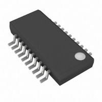
MAX4929EEEP+T Maxim Integrated Products, MAX4929EEEP+T Datasheet - Page 2

MAX4929EEEP+T
Manufacturer Part Number
MAX4929EEEP+T
Description
IC SWITCH HDMI 2:1 20-QSOP
Manufacturer
Maxim Integrated Products
Series
4000r
Datasheet
1.MAX4929EEEP.pdf
(13 pages)
Specifications of MAX4929EEEP+T
Function
Switch
Circuit
1 x 2:1
On-state Resistance
25 Ohm
Operating Temperature
-40°C ~ 85°C
Mounting Type
Surface Mount
Package / Case
20-QSOP
Lead Free Status / RoHS Status
Lead free / RoHS Compliant
HDMI 2:1 Low-Frequency Translating Switch
ABSOLUTE MAXIMUM RATINGS
(All voltages referenced to GND, unless otherwise noted.)
V+ ............................................................................-0.3V to +6V
All Pins (except GND) .............................................-0.3V to +6V
Continuous Current into Any I/O Terminal .........................25mA
Continuous Power Dissipation (T
ELECTRICAL CHARACTERISTICS
(V+ = +5V ±10%, CLP = VL = +3.3V ±10%, T
Stresses beyond those listed under “Absolute Maximum Ratings” may cause permanent damage to the device. These are stress ratings only, and functional
operation of the device at these or any other conditions beyond those indicated in the operational sections of the specifications is not implied. Exposure to
absolute maximum rating conditions for extended periods may affect device reliability.
2
POWER SUPPLY
V+ Supply Current
V+ Supply Current
VL Supply Current
CLP Supply Current
ANALOG SWITCH
On-Resistance
On-Resistance Match Between
Channels
On-Resistance Flatness
Off-Leakage Current
On-Leakage Current
Output Clamped Voltage
SWITCH DYNAMIC CHARACTERISTICS
SCL_, SDA_ Off-Capacitance
SCL_, SDA_ On-Capacitance
Bandwidth
Crosstalk
Off-Isolation
LOGIC INPUT (HPIR1, HPIR2)
Input Logic-Low Voltage
Input Logic-High Voltage
Input Logic Leakage
20-Pin QSOP (derate 9.1mW/°C above +70°C) ..........727mW
20-Pin TQFN (derate 16.9mW/°C above +70°C) ......1356mW
_______________________________________________________________________________________
PARAMETER
A
= +70°C)
V
V
C
C
R
I
C
R
I
C
I
SYMBOL
SCL_(OFF),
I
SDA_(OFF)
OV C ( S C L O) ,
OV C ( S D A O)
SCL_(ON),
SDA_(ON)
SCL_(OFF),
SDA_(OFF)
ON(SCL_),
SCL_(ON),
ON(SDA_)
SDA_(ON)
R
ΔR
V
I
V
BW
I
V
I
CLP
FLAT
V
INL
I+
I+
ISO
VL
CT
IH
IL
ON
A
= T
V+ = 5.5V, VL = CLP = 3.6V
V+ = 0V, VL = CLP = 0V, V
V+ = 5.5V, VL = CLP = 3.6V
V+ = 5.5V, VL = CLP = 3.6V
V+ = 4.5V, CLP = 3V, V
1.5V; I
V+ = 4.5V, CLP = 3V, V
1.5V; I
V+ = 4.5V, CLP = 3V, V
1.5V; I
V+ = 5.5V, V
HIZ1 = HIZ2 = 0V or VL (Note 1)
V+ = 5.5V, V
(Note 1)
V+ = 5V, CLP = 3.3V, VL = 5V, R
(Note 2)
V+ = 5V, T
V+ = 5V, T
R
R
R
V+ = 4.5V
V+ = 5.5V
MIN
S
S
S
= R
= R
= R
to T
SCL_
SCL_
SCL_
L
L
L
= 50Ω, C
= 50Ω, f = 1MHz, Figure 2 (Note 3)
= 50Ω, f = 1MHz, Figure 2 (Note 4)
MAX
A
A
or I
or I
or I
= +25°C, Figure 1
= +25°C, Figure 1
SCL_
SCL_
, unless otherwise noted. Typical values are at T
SDA_
SDA_
SDA_
CONDITIONS
L
or V
or V
= 10pF
Operating Temperature Range ...........................-40°C to +85°C
Storage Temperature Range .............................-65°C to +150°C
Junction Temperature ......................................................+150°C
Lead Temperature (soldering, 10s) .................................+300°C
= ±10mA
= ±10mA
= ±10mA
SDA_
SDA_
SCL_
SCL_
SCL_
HPIR_
= 0V, 5.5V;
= 0V, 5.5V
or V
or V
or V
SDA_
SDA_
SDA_
P
= +5.5V
= 1kΩ
= 0 to
= 0 to
= 0 to
MIN
3.8
-5
-5
TYP
0.01
-75
-70
3.3
10
20
30
40
3
2
A
= +25°C.)
MAX
200
+5
+5
0.8
25
13
8
1
1
8
1
UNITS
MHz
µA
µA
µA
µA
µA
µA
pF
pF
dB
dB
µA
Ω
Ω
Ω
V
V
V


