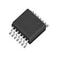
LM6584MT National Semiconductor, LM6584MT Datasheet - Page 12

LM6584MT
Manufacturer Part Number
LM6584MT
Description
Manufacturer
National Semiconductor
Type
General Purpose Amplifierr
Datasheet
1.LM6584MT.pdf
(16 pages)
Specifications of LM6584MT
Rail/rail I/o Type
Rail to Rail Input/Output
Number Of Elements
4
Unity Gain Bandwidth Product
15.3MHz
Slew Rate
11V/us
Common Mode Rejection Ratio
72dB
Input Offset Voltage
4mV
Input Bias Current
1uA
Single Supply Voltage (typ)
9/12V
Dual Supply Voltage (typ)
Not RequiredV
Voltage Gain In Db
106dB
Power Supply Rejection Ratio
75dB
Power Supply Requirement
Single
Shut Down Feature
No
Single Supply Voltage (min)
5V
Single Supply Voltage (max)
13V
Dual Supply Voltage (min)
Not RequiredV
Dual Supply Voltage (max)
Not RequiredV
Technology
Bipolar
Operating Temp Range
-40C to 85C
Operating Temperature Classification
Industrial
Mounting
Surface Mount
Pin Count
14
Package Type
TSSOP
Lead Free Status / Rohs Status
Not Compliant
Available stocks
Company
Part Number
Manufacturer
Quantity
Price
Company:
Part Number:
LM6584MT
Manufacturer:
NS
Quantity:
1 537
Part Number:
LM6584MT
Manufacturer:
NS/国半
Quantity:
20 000
Part Number:
LM6584MT.
Manufacturer:
NS/国半
Quantity:
20 000
Company:
Part Number:
LM6584MTX
Manufacturer:
MAXIM
Quantity:
2 590
Part Number:
LM6584MTX
Manufacturer:
NS/国半
Quantity:
20 000
www.national.com
TFT Display Application
8KHz to160KHz, which is much lower than the gain band-
width of most op amps. As a result, the V
little phase lag when op amp loop gain is unity, and this
allows the V
measuring the small-signal bandwidth of the LM6584 with
the RC load of Figure 4. When driving an RC load of 50nF
and 20Ω, the LM6584 has a unity gain frequency of 6.12MHz
with 41.5˚C of phase margin. If the load capacitor is in-
creased to 200nF and the resistance remains 20Ω, the unity
gain frequency is virtually unchanged: 6.05MHz with 42.9˚C
of phase margin.
A V
the op amp’s maximum output current, not by its slew rate.
This is easily shown by calculating how much output current
is required to slew a 50nF load capacitance at the LM6584
slew rate of 14V/µs:
700mA exceeds the maximum current specification for the
LM6584 and almost all other op amps, confirming that a
V
order to minimize V
V
Figure 5 is a common test circuit used for measuring V
driver response time. The RC network of R
COM
COM
COM
FIGURE 4. V
driver’s speed is limited by its peak output current. In
Driver must supply large values of output current.
Driver’s large-signal response time is determined by
FIGURE 5. V
COM
Driver to remain stable. This was verified by
I
COM
OUT
COM
= 14V/µs x 50nF
Driver with Simplified Load
COM
= 700mA
transients, the op amp used as a
Driver Test Circuit
COM
(Continued)
L1
load adds very
to R
20059230
L3
20059229
and C
COM
1
12
to C
network is a gross simplification of what the actual imped-
ance is on a TFT panel. However, it does provide a useful
test for measuring the op amp’s transient response when
driving a large capacitive load. A low impedance MOSFET
driver applies a 5V square wave to V
current pulses in the RC network. Scope photos from this
circuit are shown in Figure 6 and Figure 7. Figure 6 shows
the test circuit generates positive and negative voltage
spikes with an amplitude of
both transients settle-out in approximately 2µs. As men-
tioned before, the speed at which these transients settle-out
is a function of the op amp’s peak output current. The I
trace in Figure 7 shows that the LM6584 can sink and source
peak currents of −310mA and 320mA. This ability to supply
large values of output current makes the LM6584 extremely
well suited for V
GAMMA BUFFER
Illumination in a TFT display, also referred to as grayscale, is
set by a series of discrete voltage levels that are applied to
each LCD pixel. These voltage levels are generated by
resistive DAC networks that reside inside each of the column
driver ICs. For example, a column driver with 64 Grayscale
FIGURE 7. V
FIGURE 6. V
4
models the distributed RC load of a V
SW
COM
SW
and I
and V
Driver applications.
OUT
Circuit
COM
Waveforms from V
±
3.2V at the V
Waveforms from V
SW
, generating large
COM
COM
20059231
20059232
line. This RC
COM
node, and
COM
Test
OUT


