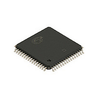
CY7C144-15AI Cypress Semiconductor Corp, CY7C144-15AI Datasheet - Page 8

CY7C144-15AI
Manufacturer Part Number
CY7C144-15AI
Description
Manufacturer
Cypress Semiconductor Corp
Datasheet
1.CY7C144-15AI.pdf
(20 pages)
Specifications of CY7C144-15AI
Density
64Kb
Access Time (max)
15ns
Sync/async
Asynchronous
Architecture
Not Required
Clock Freq (max)
Not RequiredMHz
Operating Supply Voltage (typ)
5V
Address Bus
13b
Package Type
TQFP
Operating Temp Range
-40C to 85C
Number Of Ports
2
Operating Supply Voltage (min)
4.5V
Operating Supply Voltage (max)
5.5V
Operating Temperature Classification
Industrial
Mounting
Surface Mount
Pin Count
64
Word Size
8b
Number Of Words
8K
Lead Free Status / Rohs Status
Not Compliant
Available stocks
Company
Part Number
Manufacturer
Quantity
Price
Company:
Part Number:
CY7C144-15AI
Manufacturer:
TQS
Quantity:
493
Switching Characteristics
Over the Operating Range
Notes
Document #: 38-06034 Rev. *E
READ CYCLE
t
t
t
t
t
t
t
t
t
t
t
WRITE CYCLE
t
t
t
t
t
t
t
t
t
t
t
t
8. Test conditions assume signal transition time of 3 ns or less, timing reference levels of 1.5V, input pulse levels of 0 to 3.0V, and output loading of the specified I
9. At any given temperature and voltage condition for any given device, t
10. Test conditions used are Load 3.
11. This parameter is guaranteed but not tested.
12. For information on part-to-part delay through RAM cells from writing port to reading port, refer to Read Timing with Port-to-Port Delay waveform.
RC
AA
OHA
ACE
DOE
LZOE
HZOE
LZCE
HZCE
PU
PD
WC
SCE
AW
HA
SA
PWE
SD
HD
HZWE
LZWE
WDD
DDD
Parameter
and 30-pF load capacitance.
[11]
[11]
[12]
[12]
[9, 10,11]
[9, 10,11]
[9, 10,11]
[9, 10,11]
[10,11]
[10,11]
Read Cycle Time
Address to Data Valid
Output Hold From Address
Change
CE LOW to Data Valid
OE LOW to Data Valid
OE Low to Low Z
OE HIGH to High Z
CE LOW to Low Z
CE HIGH to High Z
CE LOW to Power-Up
CE HIGH to Power-Down
Write Cycle Time
CE LOW to Write End
Address Set-Up to Write End
Address Hold From Write End
Address Set-Up to Write Start
Write Pulse Width
Data Set-Up to Write End
Data Hold From Write End
R/W LOW to High Z
R/W HIGH to Low Z
Write Pulse to Data Delay
Write Data Valid to Read Data
Valid
[8]
Description
Min
15
15
12
12
12
10
3
3
3
0
2
0
3
0
7C144-15
7C145-15
HZCE
Max
15
15
10
10
10
15
10
30
25
is less than t
Min
25
25
20
20
20
15
3
3
3
0
2
0
0
3
7C144-25
7C145-25
LZCE
and t
Max
25
25
15
15
15
25
15
50
30
HZOE
is less than t
Min
35
35
30
30
25
15
3
3
3
0
2
0
0
3
7C144-35
7C145-35
LZOE
Max
CY7C144, CY7C145
35
35
20
20
20
35
20
60
35
.
Min
55
55
45
45
40
25
3
3
3
0
2
0
0
3
7C144-55
7C145-55
Max
55
55
25
25
70
40
25
25
55
Page 8 of 20
Unit
ns
ns
ns
ns
ns
ns
ns
ns
ns
ns
ns
ns
ns
ns
ns
ns
ns
ns
ns
ns
ns
ns
ns
OI
/I
OH
[+] Feedback


