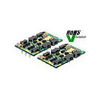
Q48T20050-NBB0 POWER ONE, Q48T20050-NBB0 Datasheet - Page 9

Q48T20050-NBB0
Manufacturer Part Number
Q48T20050-NBB0
Description
Manufacturer
POWER ONE
Type
Step Downr
Datasheet
1.Q48T20050-NBB0.pdf
(15 pages)
Specifications of Q48T20050-NBB0
Number Of Outputs
1
Output Current
20A
Input Voltage
48V
Output Voltage
5V
Screening Level
Industrial
Product Length (mm)
36.83mm
Product Height (mm)
6.52mm
Product Depth (mm)
58.42mm
Mounting Style
Through Hole
Pin Count
8
Package / Case
Quarter-Brick
Lead Free Status / Rohs Status
Not Compliant
Characterization
General Information
The converter has been characterized for many operational
aspects, to include thermal derating (maximum load current
as a function of ambient temperature and airflow) for vertical
and horizontal mounting, efficiency, start-up and shutdown
parameters, output ripple and noise, transient response to
load step-change, overload and short circuit.
The following pages contain specific plots or waveforms as-
sociated with the converter. Additional comments for specific
data are provided below.
Test Conditions
All data presented were taken with the converter soldered to
a test board, specifically a 0.060” thick printed wiring board
(PWB) with four layers. The top and bottom layers were not
metalized. The two inner layers, comprising two-ounce cop-
per, were used to provide traces for connectivity to the con-
verter.
The lack of metalization on the outer layers as well as the
limited thermal connection ensured that heat transfer from
the converter to the PWB was minimized. This provides a
worst-case but consistent scenario for thermal derating pur-
poses.
All measurements requiring airflow were made in Power-
One’s vertical and horizontal wind tunnel facilities using In-
frared (IR) thermography and thermocouples for thermome-
try.
Ensuring components on the converter do not exceed their
ratings is important to maintaining high reliability. If one an-
ticipates operating the converter at or close to the maximum
loads specified in the derating curves, it is prudent to check
actual operating temperatures in the application. Thermo-
graphic imaging is preferable; if this capability is not avail-
able, then thermocouples may be used. Power-One recom-
mends the use of AWG #40 gauge thermocouples to ensure
measurement accuracy. Careful routing of the thermocouple
leads will further minimize measurement error. Refer to Fig-
ure 28 for optimum measuring thermocouple location.
Thermal Derating
Load current vs. ambient temperature and airflow rates are
given in Figs. 10-13 for through-hole and surface mount ver-
NOV 07, 2003 revised to NOV 20, 2006
Q48T20050 and Q48S20050 DC-DC Converter Data Sheet
Page 9 of 15
36-75 VDC Input; 5.0 VDC @ 20A Output
sion. Ambient temperature was varied between 25°C and
85°C, with airflow rates from 30 to 500 LFM (0.15 to 2.5
m/s), and vertical and horizontal converter mounting.
For each set of conditions, the maximum load current was
defined as the lowest of:
(i) The output current at which either any FET junction tem-
perature did not exceed a maximum specified temperature
(120°C) as indicated by the thermographic image, or
(ii) The nominal rating of the converter (20 A)
During normal operation, derating curves with maximum FET
temperature less than or equal to 120°C should not be ex-
ceeded. Temperature on the PCB at the thermocouple loca-
tion shown in Fig. 28 should not exceed 118°C in order to
operate inside the derating curves.
Efficiency
Efficiency vs. load current plots are shown in Figs. 14 and 16
for ambient temperature of 25ºC, airflow rate of 300 LFM
(1.5 m/s), both vertical and horizontal orientations, and input
voltages of 36 V, 48 V and 72 V. Also, plots of efficiency vs.
load current, as a function of ambient temperature with Vin =
48 V, airflow rate of 200 LFM (1 m/s) are shown for both a
vertically and horizontally mounted converter in Figs. 15 and
17, respectively.
Start-up
Output voltage waveforms, during the turn-on transient using
the ON/OFF pin for full rated load currents (resistive load)
are shown without and with 10,000 μ F load capacitance in
Figs. 18 and 19, respectively.
Ripple and Noise
Figure 22 shows the output voltage ripple waveform, meas-
ured at full rated load current with a 10 µF tantalum and 1 µF
ceramic capacitor across the output. Note that all output
voltage waveforms are measured across a 1 μ F ceramic ca-
pacitor.
The input reflected ripple current waveforms are obtained
using the test setup shown in Fig 23. The corresponding
waveforms are shown in Figs. 24 and 25.
www.power-one.com


