DS3691MX National Semiconductor, DS3691MX Datasheet

DS3691MX

Manufacturer Part Number
DS3691MX
Description
Manufacturer
National Semiconductor
Datasheet

Specifications of DS3691MX

Interface Circuit Standard 1
RS-422
Number Of Receivers
Not Required
Number Of Transmitters
2@RS-422/4@RS-423
Number Of Transceivers
Not Required
Data Transmission Topology
Multidrop
Receiver Signal Type
Not Required
Single Supply Voltage (typ)
Not RequiredV
Single Supply Voltage (min)
Not RequiredV
Single Supply Voltage (max)
Not RequiredV
Dual Supply Voltage (typ)
±5V
Dual Supply Voltage (min)
±4.75V
Dual Supply Voltage (max)
±5.25V
Supply Current
30mA
Power Supply Requirement
Dual
Operating Temp Range
0C to 70C
Operating Temperature Classification
Commercial
Mounting
Surface Mount
Pin Count
16
Package Type
SOIC N
Lead Free Status / Rohs Status
Not Compliant

Available stocks

Company
Part Number
Manufacturer
Quantity
Price
Part Number:
DS3691MX
Manufacturer:
NS
Quantity:
2 139
Part Number:
DS3691MX
Manufacturer:
NS/国半
Quantity:
20 000
Part Number:
DS3691MX
Manufacturer:
NS
Quantity:
5 413
Part Number:
DS3691MX
Quantity:
2 400
Part Number:
DS3691MX/NOPB
Manufacturer:
TI
Quantity:
12 304
Part Number:
DS3691MX/NOPB
Manufacturer:
TI/德州仪器
Quantity:
20 000
© 2004 National Semiconductor Corporation
DS1691A/DS3691
(RS-422/RS-423) Line Drivers with TRI-STATE
General Description
The DS1691A/DS3691 are low power Schottky TTL line
drivers designed to meet the requirements of EIA standards
RS-422 and RS-423. They feature 4 buffered outputs with
high source and sink current capability with internal short
circuit protection. A mode control input provides a choice of
operation either as 4 single-ended line drivers or 2 differen-
tial line drivers. A rise time control pin allows the use of an
external capacitor to slow the rise time for suppression of
near end crosstalk to other receivers in the cable. Rise time
capacitors are primarily intended for waveshaping output
signals in the single-ended driver mode. Multipoint applica-
tions in differential mode with waveshaping capacitors is not
allowed.
With the mode select pin low, the DS1691A/DS3691 are
dual-differential line drivers with TRI-STATE outputs. They
feature
mode and 0V output unbalance when operated with
supply.
Connection Diagrams
Ordering Information
TRI-STATE
®
±
is a registered trademark of National Semiconductor Corporation.
10V output common-mode range in TRI-STATE
Order Number
DS3691M
DS3691N
For Complete Military Product Specifications, refer to the appropriate SMD or MDS.
DS1691AJ/883
With Mode Select LOW
(RS-422 Connection)
Top View
DS005783
00578301
Package Type
Ceramic DIP
SO Package
±
Molded DIP
5V
Features
n Dual RS-422 line driver with mode pin low, or quad
n TRI-STATE outputs in RS-422 mode
n Short circuit protection for both source and sink outputs
n Outputs will not clamp line with power off or in
n 100Ω transmission line drive capability
n Low I
n Low current PNP inputs compatible with TTL, MOS and
n Pin compatible with AM26LS30
RS-423 line driver with mode pin high
TRI-STATE
CMOS
RS-422: I
RS-423: I
CC
and I
CC
CC
EE
With Mode Select HIGH
(RS-423 Connection)
= 9 mA/driver typ
= 4.5 mA/driver typ:
power consumption
I
NS Package Number
EE
Top View
= 2.5 mA/driver typ
M16A
N16E
J16A
®
Outputs
www.national.com
00578302
July 1998

Related parts for DS3691MX

DS3691MX Summary of contents

Page 1

... DS3691N For Complete Military Product Specifications, refer to the appropriate SMD or MDS. DS1691AJ/883 TRI-STATE ® registered trademark of National Semiconductor Corporation. © 2004 National Semiconductor Corporation Features n Dual RS-422 line driver with mode pin low, or quad RS-423 line driver with mode pin high ...

Page 2

... Absolute Maximum Ratings If Military/Aerospace specified devices are required, please contact the National Semiconductor Sales Office/ Distributors for availability and specifications. Supply Voltage Maximum Power Dissipation (Note 1) at 25˚C Cavity Package Molded DIP Package SO Package Input Voltage Output Voltage (Power OFF) Storage Temperature ...

Page 3

AC Electrical Characteristics T = 25˚C A Symbol Parameter RS-422 CONNECTION 5V, MODE SELECT = 0. Output Rise Time r t Output Fall Time f t Output Propagation Delay PDH t Output Propagation Delay PDL t ...

Page 4

AC Electrical Characteristics T = 25˚C A Symbol Parameter t Output Propagation Delay PDH t Output Propagation Delay PDL AC Test Circuits and Switching Time Waveforms www.national.com (Note 6) (Continued) Conditions R = 450Ω 500 pF ...

Page 5

AC Test Circuits and Switching Time Waveforms FIGURE 3. Rise Time Control for RS-423 00578309 FIGURE 4. TRI-STATE Delays 5 (Continued) 00578307 00578308 www.national.com 00578310 ...

Page 6

Switching Waveforms Truth Table Operation RS-422 RS-423 Typical Application Information www.national.com 00578311 FIGURE 5. Typical Output Voltage Inputs Mode A (D) B ( TRI-STATE ...

Page 7

Typical Application Information Differential Application with Rise Time Control *Note: Controlled edge allows longer stub lengths. Multiple Drivers are NOT allowed. (Continued) Fully Loaded RS-423 Interface Dual RS-423 Inverting Driver 7 00578315 00578316 00578317 www.national.com ...

Page 8

Typical Rise Time Control Characteristics (RS-423 Mode) www.national.com Rise Time vs External Capacitor 00578312 8 ...

Page 9

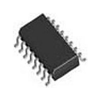
Physical Dimensions inches (millimeters) unless otherwise noted Ceramic Dual-In-Line Package (J) Order Number DS1691AJ/883 NS Package Number J16A SO Package (M) Order Number DS3691M NS Package Number M16A 9 www.national.com ...

Page 10

... BANNED SUBSTANCE COMPLIANCE National Semiconductor certifies that the products and packing materials meet the provisions of the Customer Products Stewardship Specification (CSP-9-111C2) and the Banned Substances and Materials of Interest Specification (CSP-9-111S2) and contain no ‘‘Banned Substances’’ as defined in CSP-9-111S2. ...

Related keywords