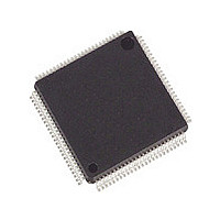
M30624FGPGP Renesas Electronics America, M30624FGPGP Datasheet - Page 69

M30624FGPGP
Manufacturer Part Number
M30624FGPGP
Description
Manufacturer
Renesas Electronics America
Datasheet
1.M30624FGPGP.pdf
(103 pages)
Specifications of M30624FGPGP
Cpu Family
M16C
Device Core Size
16/32Bit
Frequency (max)
24MHz
Interface Type
I2C/IEBus/UART
Program Memory Type
Flash
Program Memory Size
256KB
Total Internal Ram Size
20KB
# I/os (max)
87
Number Of Timers - General Purpose
11
Operating Supply Voltage (typ)
5V
Operating Supply Voltage (max)
5.5V
Operating Supply Voltage (min)
3.3V
On-chip Adc
26-chx10-bit
On-chip Dac
2-chx8-bit
Instruction Set Architecture
CISC
Mounting
Surface Mount
Pin Count
100
Package Type
LQFP
Lead Free Status / Rohs Status
Compliant
Available stocks
Company
Part Number
Manufacturer
Quantity
Price
Company:
Part Number:
M30624FGPGP
Manufacturer:
RENESAS
Quantity:
14
Part Number:
M30624FGPGP
Manufacturer:
RENESAS/瑞萨
Quantity:
20 000
Company:
Part Number:
M30624FGPGP#D3C
Manufacturer:
Renesas Electronics America
Quantity:
10 000
Company:
Part Number:
M30624FGPGP#D5C
Manufacturer:
Renesas Electronics America
Quantity:
10 000
Company:
Part Number:
M30624FGPGP#U3C
Manufacturer:
AVX
Quantity:
40 000
Company:
Part Number:
M30624FGPGP#U3C
Manufacturer:
Renesas
Quantity:
1 200
Company:
Part Number:
M30624FGPGP#U3C
Manufacturer:
Renesas Electronics America
Quantity:
10 000
Company:
Part Number:
M30624FGPGP#U5
Manufacturer:
RENESAS
Quantity:
1
Company:
Part Number:
M30624FGPGP#U5C
Manufacturer:
RENESAS
Quantity:
1 467
M16C/62P Group (M16C/62P, M16C/62PT)
Rev.2.41
REJ03B0001-0241
Timing Requirements
(V
CC1
Table 5.32
NOTES:
Table 5.33
NOTES:
t
t
t
t
t
t
t
t
t
t
t
t
t
t
c
w(H)
w(L)
r
f
ac1(RD-DB)
ac2(RD-DB)
ac3(RD-DB)
su(DB-RD)
su(RDY-BCLK)
su(HOLD-BCLK)
h(RD-DB)
h(BCLK-RDY)
h(BCLK-HOLD)
Symbol
Symbol
1. The condition is V
2. Calculated according to the V
3. Calculated according to the V
4. Calculated according to the V
1. Calculated according to the BCLK frequency as follows:
2. Calculated according to the BCLK frequency as follows:
3. Calculated according to the BCLK frequency as follows:
= V
CC2
Jan 10, 2006
--------------------------------------- -
20 V
–
----------------------- - 60 ns
f BCLK
0.5x10
(
----------------------------------- - 60 ns
(
----------------------------------- - 60 ns
(
--------------------------------------- -
20 V
10
n 0.5
n 0.5
f BCLK
f BCLK
= 3V, V
×
–
–
(
(
×
×
External Clock Input Cycle Time
External Clock Input HIGH Pulse Width
External Clock Input LOW Pulse Width
External Clock Rise Time
External Clock Fall Time
10
Data Input Access Time (for setting with no wait)
Data Input Access Time (for setting with wait)
Data Input Access Time (when accessing multiplex bus area)
Data Input Setup Time
RDY Input Setup Time
HOLD Input Setup Time
Data Input Hold Time
RDY Input Hold Time
HOLD Input Hold Time
V
10
C C1
9
External Clock Input (XIN input)
C C2
C C1
Memory Expansion Mode and Microprocessor Mode
–
) x10
)
) x10
6
–
–
6
–
)
)
–
+
SS
44
9
9
44
45
[
–
–
×
= 0V, at T
[ns]
0.4
]
[ns]
[
[
CC1
Page 67 of 96
[ns]
]
]
=V
CC2
n is ”2” for 1-wait setting, “3” for 2-wait setting and “4” for 3-wait setting.
n is “2” for 2-wait setting, “3” for 3-wait setting.
opr
=2.7 to 3.0V.
= −20 to 85°C / −40 to 85°C unless otherwise specified)
CC1
CC1
CC1
Parameter
Parameter
voltage as follows:
voltage as follows:
voltage as follows:
(1)
(NOTE 2)
(NOTE 3)
(NOTE 3)
Min.
Min.
50
40
50
0
0
0
V
Standard
Standard
CC1
5. Electrical Characteristics
(NOTE 4)
(NOTE 4)
(NOTE 1)
(NOTE 2)
(NOTE 3)
Max.
Max.
=V
CC2
Unit
Unit
=3V
ns
ns
ns
ns
ns
ns
ns
ns
ns
ns
ns
ns
ns
ns


