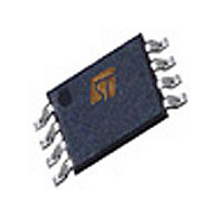
M93C66-WDW6T STMicroelectronics, M93C66-WDW6T Datasheet - Page 18

M93C66-WDW6T
Manufacturer Part Number
M93C66-WDW6T
Description
Manufacturer
STMicroelectronics
Datasheet
1.M93C66-WDW6T.pdf
(37 pages)
Specifications of M93C66-WDW6T
Density
4Kb
Interface Type
Serial (Microwire)
Organization
512x8/256x16
Frequency (max)
2MHz
Write Protection
No
Data Retention
40Year
Operating Supply Voltage (typ)
3.3/5V
Package Type
TSSOP
Operating Temp Range
-40C to 85C
Supply Current
2mA
Operating Supply Voltage (min)
2.5V
Operating Supply Voltage (max)
5.5V
Operating Temperature Classification
Industrial
Mounting
Surface Mount
Pin Count
8
Lead Free Status / Rohs Status
Not Compliant
Available stocks
Company
Part Number
Manufacturer
Quantity
Price
Company:
Part Number:
M93C66-WDW6T
Manufacturer:
ST
Quantity:
3 165
Part Number:
M93C66-WDW6TP
Manufacturer:
ST
Quantity:
20 000
READY/BUSY status
6
7
8
18/37
READY/BUSY status
While the Write or Erase cycle is underway, for a WRITE, ERASE, WRAL or ERAL
instruction, the Busy signal (Q=0) is returned whenever Chip Select input (S) is driven high.
(Please note, though, that there is an initial delay, of t
becomes available). In this state, the M93Cx6 ignores any data on the bus. When the Write
cycle is completed, and Chip Select Input (S) is driven high, the Ready signal (Q=1)
indicates that the M93Cx6 is ready to receive the next instruction. Serial Data Output (Q)
remains set to 1 until the Chip Select Input (S) is brought low or until a new start bit is
decoded.
Initial delivery state
The device is delivered with all bits in the memory array set to 1 (each byte contains FFh).
Common I/O operation
Serial Data Output (Q) and Serial Data Input (D) can be connected together, through a
current limiting resistor, to form a common, single-wire data bus. Some precautions must be
taken when operating the memory in this way, mostly to prevent a short circuit current from
flowing when the last address bit (A0) clashes with the first data bit on Serial Data Output
(Q). Please see the application note AN394 for details.
M93C86, M93C76, M93C66, M93C56, M93C46
SLSH
, before this status information


