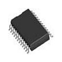
DS14C238WM National Semiconductor, DS14C238WM Datasheet - Page 4

DS14C238WM
Manufacturer Part Number
DS14C238WM
Description
Manufacturer
National Semiconductor
Datasheet
1.DS14C238WM.pdf
(5 pages)
Specifications of DS14C238WM
Data Rate
120Kbps
Interface Circuit Standard 1
EIA/TIA-232-E/V.28
Number Of Receivers
4
Number Of Transmitters
4
Number Of Transceivers
1
Data Transmission Topology
Point-to-Point
Receiver Signal Type
Single-Ended
Transmitter Signal Type
Single-Ended
Single Supply Voltage (typ)
5V
Single Supply Voltage (min)
4.5V
Single Supply Voltage (max)
5.5V
Dual Supply Voltage (typ)
Not RequiredV
Dual Supply Voltage (min)
Not RequiredV
Dual Supply Voltage (max)
Not RequiredV
Supply Current
10mA
Power Supply Requirement
Single
Operating Temp Range
0C to 70C
Operating Temperature Classification
Commercial
Mounting
Surface Mount
Pin Count
24
Package Type
SOIC W
Lead Free Status / Rohs Status
Not Compliant
Available stocks
Company
Part Number
Manufacturer
Quantity
Price
Company:
Part Number:
DS14C238WM
Manufacturer:
NS
Quantity:
169
Part Number:
DS14C238WM
Manufacturer:
NS/国半
Quantity:
20 000
Company:
Part Number:
DS14C238WMX
Manufacturer:
MAXIM
Quantity:
1 995
Part Number:
DS14C238WMX
Manufacturer:
NS/国半
Quantity:
20 000
Company:
Part Number:
DS14C238WMX/NOPB
Manufacturer:
NS
Quantity:
7 804
www.national.com
Parameter Measurement Information
Pin Descriptions
V
+5V (
V+ (pin 11) — Positive supply for TIA/EIA-232-E drivers. Recommended external capacitor: C4 = 1.0 µF (6.3V). This supply is not
intended to be loaded externally.
V− (pin 15) — Negative supply for TIA/EIA-232-E drivers. Recommended external capacitor: C3 = 1.0 µF (16V). This supply is not
intended to be loaded externally.
C1+, C1− (pins 10 and 12) — External capacitor connection pins. Recommended capacitor – 1.0 µF (6.3V).
C2+, C2− (pins 13 and 14) — External Capacitor connection pins. Recommended capacitor – 1.0 µF (16V).
D
internal pull-up resistor (500 kΩ minimum, typically 5 MΩ) pulls input to V
D
R
filter and guaranteed hysteresis of 200 mV. Unused receiver input pins may be left open. Internal input resistor (5 kΩ) pulls input
LOW, providing a failsafe HIGH output.
R
for both CMOS and TTL load conditions.
GND (pin 8) — Ground Pin.
CC
IN
OUT
IN1
OUT
1–4 (pins 5, 18, 19, and 21) — Driver input pins are TTL/CMOS compatible. Inputs of unused drivers may be left open, an
(pin 9) — Power supply pin for the device,
1–4 (pins 3, 7, 23, and 16) — Receiver input pins accept TIA/EIA-232-E input voltages (
±
1–4 (pins 4, 6, 22, and 17) — Receiver output pins are TTL/CMOS compatible. Receiver output HIGH voltage is specified
1–4 (pins 2, 1, 24, and 20) — Driver output pins conform to TIA/EIA-232-E levels.
10%).
FIGURE 4. Receiver Propagation Delays and Noise Rejection
4
(Continued)
CC
. Output will be LOW for open inputs.
±
15V). Receivers feature a noise
01128207


