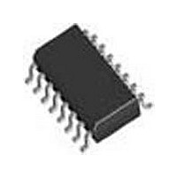
LP2953IM National Semiconductor, LP2953IM Datasheet - Page 3

LP2953IM
Manufacturer Part Number
LP2953IM
Description
Manufacturer
National Semiconductor
Datasheet
1.LP2953IM.pdf
(22 pages)
Specifications of LP2953IM
Voltage Regulator Type
Linear
Topology
LDO
Regulator Output Type
Adjustable
Polarity Type
Positive
Number Of Outputs
Single
Input Voltage (min)
-20V
Input Voltage (max)
30V
Output Voltage
1.23 to 29V
Package Type
SOIC N
Output Current
250mA
Load Regulation
0.2%
Line Regulation
0.2%
Operating Temp Range
-40C to 125C
Operating Temperature Classification
Automotive
Pin Count
16
Mounting
Surface Mount
Quiescent Current (max)
170uA
Lead Free Status / Rohs Status
Not Compliant
Available stocks
Company
Part Number
Manufacturer
Quantity
Price
Company:
Part Number:
LP2953IM
Manufacturer:
national
Quantity:
464
Part Number:
LP2953IM
Manufacturer:
NS/国半
Quantity:
20 000
Company:
Part Number:
LP2953IM-3.3
Manufacturer:
nstion
Quantity:
753
Part Number:
LP2953IMX
Manufacturer:
NS/国半
Quantity:
20 000
Company:
Part Number:
LP2953IMX-3.3/NOPB
Manufacturer:
NS
Quantity:
11 855
Company:
Part Number:
LP2953IMX-4.7/NOPB
Manufacturer:
NS
Quantity:
11 184
Company:
Part Number:
LP2953IMX/NOPB
Manufacturer:
NS
Quantity:
12 692
V
V
REGULATOR
Symbol
Symbol
Symbol
O
O
Absolute Maximum Ratings
If Military/Aerospace specified devices are required,
please contact the National Semiconductor Sales Office/
Distributors for availability and specifications.
Electrical Characteristics
operating temperature range. Limits are guaranteed by production testing or correlation techniques using standard Statistical
Quality Control (SQC) methods. Unless otherwise specified: V
4.7µF for 3.3V parts. Feedback pin is tied to V Tap pin, Output pin is tied to Output Sense pin.
3.3V Versions
5V Versions
All Voltage Options
Electrical Characteristics
Limits in standard typeface are for T
anteed by production testing or correlation techniques using standard Statistical Quality Control (SQC) methods. Unless other-
wise specified: V
Tap pin, Output pin is tied to Output Sense pin.
Storage Temperature Range
Operating Temperature Range
Lead Temp. (Soldering, 5 seconds)
Power Dissipation (Note 2)
LP2952I, LP2953I, LP2952AI,
LP2953AI, LP2952I-3.3,
LP2953I-3.3, LP2952AI-3.3,
LP2953AI-3.3
LP2953AM
Output Voltage
Output Voltage
Output Voltage Temp.
Coefficient
Output Voltage Line
Regulation
Parameter
Parameter
Parameter
IN
= V
O
(NOM) + 1V, I
1 mA ≤ I
1 mA ≤ I
Conditions
Conditions
(Note 5)
V
L
IN
J
≤ 250 mA
L
−40˚C ≤ T
= 25˚C, bold typeface applies over the full operating temperature range. Limits are guar-
≤ 250 mA
= V
L
= 1 mA, C
Internally Limited
O
(NOM) + 1V to 30V
Limits in standard typeface are for T
Conditions
−65˚C ≤ T
−55˚C ≤ T
(Note 1)
J
≤ +125˚C
Typical
L
+150˚C
+125˚C
= 2.2 µF for 5V parts and 4.7µF for 3.3V parts. Feedback pin is tied to V
260˚C
3.3
3.3
Typical
A
A
5.0
5.0
≤
≤
LP2952AI-3.3, LP2953AI-3.3
IN
3
= V
3.284
3.260
3.254
Min
LP2952AI, LP2953AI,
LP2953AM (Note 17)
Typical LP2952AI, LP2953AI,
4.975
4.940
4.930
Maximum Junction Temperature
Input Supply Voltage
Feedback Input Voltage (Note 3)
Comparator Input Voltage (Note 4)
Shutdown Input Voltage (Note 4)
Comparator Output Voltage (Note
4)
ESD Rating (Note 15)
O
Min
0.03
(NOM) + 1V, I
20
LP2952I, LP2953I, LP2952AI,
LP2953AI, LP2952I-3.3,
LP2953I-3.3, LP2952AI-3.3,
LP2953AI-3.3
LP2953AM
Min
LP2952AI-3.3,
LP2953AI-3.3,
(Notes 16, 17)
J
3.317
3.340
3.346
LP2953AM
Max
= 25˚C, bold typeface applies over the full
5.025
5.060
5.070
Max
L
= 1 mA, C
Max
100
0.1
0.2
LP2952I-3.3, LP2953I-3.3
L
3.267
3.234
3.221
4.950
4.900
4.880
LP2952I, LP2953I
= 2.2 µF for 5V parts and
Min
Min
LP2952I, LP2953I,
Min
LP2952I-3.3,
LP2953I-3.3
−0.3V to +30V
−0.3V to +30V
−0.3V to +30V
5.050
5.100
5.120
−20V to +30V
3.333
3.366
3.379
Max
−0.3V to +5V
Max
Max
150
0.2
0.4
www.national.com
+125˚C
+150˚C
2 kV
ppm/˚C
Units
Units
Units
%
V
V


