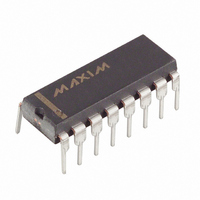
DG445DJ+ Maxim Integrated Products, DG445DJ+ Datasheet - Page 6

DG445DJ+
Manufacturer Part Number
DG445DJ+
Description
IC SWITCH QUAD SPST 16DIP
Manufacturer
Maxim Integrated Products
Datasheet
1.DG445DJ.pdf
(10 pages)
Specifications of DG445DJ+
Function
Switch
Circuit
4 x SPST - NO
On-state Resistance
85 Ohm
Voltage Supply Source
Single, Dual Supply
Voltage - Supply, Single/dual (±)
10 V ~ 30 V, ±4.5 V ~ 20 V
Operating Temperature
-40°C ~ 85°C
Mounting Type
Through Hole
Package / Case
16-DIP (0.300", 7.62mm)
Number Of Switches
Quad
Switch Configuration
SPST
On Resistance (max)
100 Ohms
On Time (max)
250 ns
Off Time (max)
170 ns
Off Isolation (typ)
60 dB
Supply Voltage (max)
30 V
Supply Voltage (min)
10 V
Supply Current
5 uA
Maximum Power Dissipation
842 mW
Maximum Operating Temperature
+ 85 C
Mounting Style
Through Hole
Minimum Operating Temperature
- 40 C
Off State Leakage Current (max)
5 nA
Lead Free Status / RoHS Status
Lead free / RoHS Compliant
Using supply voltages other than ±15V will reduce the
analog signal range. The DG444/DG445 switches oper-
Improved, Quad, SPST Analog Switches
_____________________Pin Description
• Switches are open when power is off.
• IN, D, and S should not exceed V+ or V-, even with
• Switch leakage is from each analog switch terminal
Figure 2. Switching Time
6
2, 15, 10, 7
3, 14, 11, 6
1, 16, 9, 8
the power off.
to V+ or V-, not to other switch terminals.
DIP/SO
_______________________________________________________________________________________
12
13
—
4
5
SWITCH
OUTPUT
LOGIC
INPUT
PIN
+3V
0V
0V
Operation with Supply Voltages
15, 14, 7, 6
16, 13, 8, 5
THIN QFN
LOGIC INPUT WAVEFORM IS INVERTED FOR SWITCHES
THAT HAVE THE OPPOSITE LOGIC SENSE.
1, 12, 9 4
Applications Information
EP
10
11
2
3
V
t
ON
OUT
50%
0.8 x V
IN1–IN4
D1–D4
NAME
S1–S4
GND
PAD
VL
V+
V-
OUT
General Operation
Other than ±15V
t
OFF
Logic Control
Inputs
Drain Outputs
Source Outputs
Negative-Supply
Voltage Input
Ground
Logic-Supply
Voltage Input
Positive-Supply-
Voltage
Input—Connected
to Substrate
Exposed Pad
Connect Pad to V+
t f < 20ns
t r < 20ns
FUNCTION
0.8 x V
OUT
SWITCH
LOGIC
INPUT
INPUT
ate with ±4.5V to ±20V bipolar supplies or with a +10V
to +30V single supply; connect V- to 0V when operating
with a single supply. Also, all device types can operate
with unbalanced supplies such as +24V and -5V. V
must be connected to +5V to be TTL compatible, or to
V+ for CMOS-logic level inputs. The Typical Operating
Characteristics graphs show typical on-resistance with
±20V, ±15V, ±10V, and ±5V supplies. (Switching times
increase by a factor of two or more for operation at ±5V.)
Proper power-supply sequencing is recommended
for all CMOS devices. Do not exceed the absolute
maximum ratings because stresses beyond the list-
ed ratings may cause permanent damage to the
devices. Always sequence V+ on first, followed by
V
ing is not possible, add two small, external signal
diodes in series with supply pins for overvoltage
protection (Figure 1). Adding diodes reduces the
analog signal range to 1V below V+ and 1V above
V-, but low switch resistance and low leakage char-
acteristics are unaffected. Device operation is
unchanged, and the difference between V+ and V-
should not exceed +44V.
Figure 1. Overvoltage Protection Using External Blocking Diodes
+3V
L
, V-, and logic inputs. If power-supply sequenc-
C
L
INCLUDES FIXTURE AND STRAY CAPACITANCE.
IN
D
V
REPEAT TEST FOR CHANNELS 2, 3, AND 4.
g
GND
+5V
V
L
V
OUT
= V
D
(
S
R
+15V
-15V
L
Overvoltage Protection
V+
V-
+ r
R
S
DS(ON)
L
V+
V-
)
R
L
DG444
DG445
D
C
L
V
OUT
L


