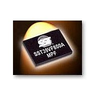
SST39VF800A-70-4C-EK Microchip Technology, SST39VF800A-70-4C-EK Datasheet - Page 2

SST39VF800A-70-4C-EK
Manufacturer Part Number
SST39VF800A-70-4C-EK
Description
Flash 512K X 16 70ns
Manufacturer
Microchip Technology
Datasheet
1.SST39VF200A-70-4C-EKE.pdf
(31 pages)
Specifications of SST39VF800A-70-4C-EK
Data Bus Width
16 bit
Memory Type
NOR
Memory Size
8 Mbit
Architecture
Sectored
Interface Type
CFI
Access Time
70 ns
Supply Voltage (max)
3.6 V
Supply Voltage (min)
2.7 V
Maximum Operating Current
30 mA
Operating Temperature
+ 70 C
Mounting Style
SMD/SMT
Package / Case
TSOP-48
Organization
512 KB x 16
Lead Free Status / Rohs Status
No RoHS Version Available
Available stocks
Company
Part Number
Manufacturer
Quantity
Price
Company:
Part Number:
SST39VF800A-70-4C-EK
Manufacturer:
SST
Quantity:
255
Company:
Part Number:
SST39VF800A-70-4C-EKE
Manufacturer:
SST
Quantity:
1 315
Part Number:
SST39VF800A-70-4C-EKE
Manufacturer:
SST
Quantity:
20 000
Part Number:
SST39VF800A-70-4C-EKE-T
Manufacturer:
SST
Quantity:
20 000
Data Sheet
To meet surface mount requirements, the SST39LF200A/
400A/800A and SST39VF200A/400A/800A are offered in
48-lead TSOP packages and 48-ball TFBGA packages as
well as Micro-Packages. See Figures 2, 3, and 4 for pin
assignments.
Device Operation
Commands are used to initiate the memory operation func-
tions of the device. Commands are written to the device
using standard microprocessor write sequences. A com-
mand is written by asserting WE# low while keeping CE#
low. The address bus is latched on the falling edge of WE#
or CE#, whichever occurs last. The data bus is latched on
the rising edge of WE# or CE#, whichever occurs first.
Read
The Read operation of the SST39LF200A/400A/800A and
SST39VF200A/400A/800A is controlled by CE# and OE#,
both have to be low for the system to obtain data from the
outputs. CE# is used for device selection. When CE# is
high, the chip is deselected and only standby power is con-
sumed. OE# is the output control and is used to gate data
from the output pins. The data bus is in high impedance
state when either CE# or OE# is high. Refer to the Read
cycle timing diagram for further details (Figure 5).
Word-Program Operation
The SST39LF200A/400A/800A and SST39VF200A/400A/
800A are programmed on a word-by-word basis. Before
programming, the sector where the word exists must be
fully erased. The Program operation is accomplished in
three steps. The first step is the three-byte load sequence
for Software Data Protection. The second step is to load
word address and word data. During the Word-Program
operation, the addresses are latched on the falling edge of
either CE# or WE#, whichever occurs last. The data is
latched on the rising edge of either CE# or WE#, whichever
occurs first. The third step is the internal Program operation
which is initiated after the rising edge of the fourth WE# or
CE#, whichever occurs first. The Program operation, once
initiated, will be completed within 20 µs. See Figures 6 and
7 for WE# and CE# controlled Program operation timing
diagrams and Figure 18 for flowcharts. During the Program
operation, the only valid reads are Data# Polling and Tog-
gle Bit. During the internal Program operation, the host is
free to perform additional tasks. Any commands issued
during the internal Program operation are ignored.
©2010 Silicon Storage Technology, Inc.
SST39VF200A / SST39VF400A / SST39VF800A
SST39LF200A / SST39LF400A / SST39LF800A
2 Mbit / 4 Mbit / 8 Mbit Multi-Purpose Flash
2
Sector/Block-Erase Operation
The Sector- (or Block-) Erase operation allows the system
to erase the device on a sector-by-sector (or block-by-
block)
SST39VF200A/400A/800A offers both Sector-Erase and
Block-Erase mode. The sector architecture is based on
uniform sector size of 2 KWord. The Block-Erase mode is
based on uniform block size of 32 KWord. The Sector-
Erase operation is initiated by executing a six-byte com-
mand sequence with Sector-Erase command (30H) and
sector address (SA) in the last bus cycle. The Block-Erase
operation is initiated by executing a six-byte command
sequence with Block-Erase command (50H) and block
address (BA) in the last bus cycle. The sector or block
address is latched on the falling edge of the sixth WE#
pulse, while the command (30H or 50H) is latched on the
rising edge of the sixth WE# pulse. The internal Erase
operation begins after the sixth WE# pulse. The End-of-
Erase operation can be determined using either Data#
Polling or Toggle Bit methods. See Figures 11 and 12 for
timing waveforms. Any commands issued during the Sec-
tor- or Block-Erase operation are ignored.
Chip-Erase Operation
The SST39LF200A/400A/800A and SST39VF200A/400A/
800A provide a Chip-Erase operation, which allows the
user to erase the entire memory array to the “1” state. This
is useful when the entire device must be quickly erased.
The Chip-Erase operation is initiated by executing a six-
byte command sequence with Chip-Erase command (10H)
at address 5555H in the last byte sequence. The Erase
operation begins with the rising edge of the sixth WE# or
CE#, whichever occurs first. During the Erase operation,
the only valid read is Toggle Bit or Data# Polling. See Table
4 for the command sequence, Figure 10 for timing diagram,
and Figure 21 for the flowchart. Any commands issued dur-
ing the Chip-Erase operation are ignored.
Write Operation Status Detection
The SST39LF200A/400A/800A and SST39VF200A/400A/
800A provide two software means to detect the completion
of a write (Program or Erase) cycle, in order to optimize the
system write cycle time. The software detection includes
two status bits: Data# Polling (DQ
The End-of-Write detection mode is enabled after the rising
edge of WE#, which initiates the internal Program or Erase
operation.
basis.
The
SST39LF200A/400A/800A
7
) and Toggle Bit (DQ
S71117-13-000
and
11/10
6
).


