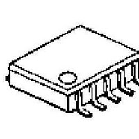
NJU7043M NJR, NJU7043M Datasheet - Page 2

NJU7043M
Manufacturer Part Number
NJU7043M
Description
Op Amps Dual High Current
Manufacturer
NJR
Datasheet
1.NJU7043M.pdf
(2 pages)
Specifications of NJU7043M
Number Of Channels
2
Voltage Gain Db
90 dB
Common Mode Rejection Ratio (min)
42 dB
Input Offset Voltage
10 mV
Operating Supply Voltage
3 V, 5 V
Supply Current
1 mA
Maximum Power Dissipation
300 mW
Maximum Operating Temperature
+ 85 C
Mounting Style
SMD/SMT
Package / Case
DMP-8
Minimum Operating Temperature
- 40 C
Lead Free Status / Rohs Status
Details
Available stocks
Company
Part Number
Manufacturer
Quantity
Price
NJU7043
PRELIMINARY
Supply Voltage
Power Dissipation
Operating Temperature Range
Storage Temperature Range
(Note) CMR is represented by either CMR+ or CMR- which has lower value.
Supply Voltage
Operating Current
Input Offset Voltage
Input Bias Current
Input Offset Current
Voltage Gain
Common Mode Rejection Ratio
Supply Voltage Rejection Ratio
H Level Output Voltage 1
L Level Output Voltage 1
H Level Output Voltage 2
L Level Output Voltage 2
Input Common Mode Voltage Range
Unity Gain Bandwidth
Total Harmonic Distortion
Equivalent Input Noise Voltage
Slew Rate
ABSOLUTE MAXIMUM RATINGS
RECOMMENDED OPERATION CONDITION
ELECTRICAL CHARACTERISTICS
AC CHARACTERISTICS
DC CHARACTERISTICS
TRANSIENT CHARACTERISTICS
PARAMETER
CMR+ is measured with 1.5V V
PARAMETER
PARAMETER
PARAMETER
PARAMETER
SYMBOL
V
DD
SYMBOL
Topr
Tstg
CM
V
P
I
V
I
I
A
CM R
S VR
V
V
V
V
V
G B
T HD
e
SR
SYMBOL
SYMBOL
SYMBOL
DD
D D
B
I O
D
n
I O
V
O H 1
O L 1
O H 2
O L 2
I C M
3V and CMR- is measured with 0V V
1.8 to 5.0
RATING
500 (DIP8)
250 (SSOP8)
300 (DMP8)
320 (TVSP8)
-55 to +125
-40 to +85
No Signal, Dual Circuits
R
0 V
2.4V V
R
R
R
R
CMR>45dB
R
f=1kHz , Vin=1Vpp , A
f=1kHz
R
RATING
L
L
L
L
L
L
L
=10k
=10k
=10k
=600
=600
=10k
=10k
5.5
CM
TEST CONDITION
TEST CONDITION
TEST CONDITION
1.5V,1.5 V
(Ta=25 C)
DD
(Ta=25 C)
5.0V, V
UNIT
V
UNIT
CM
mW
CM
v
=0dB
V
C
C
=V
3.0V(Note)
DD
/2
(Note 1)
than 5.5V, the input voltage must not
over the V
specified.
(Note 2)
connected between V
to the stabilized operation for the
circuit.
If the supply voltage (V
Decoupling capacitor should be
CM
[CAUTION]
given for information , without any guarantee
as regards either mistakes or omissions. The
application circuits in this databook are
described only to show representative usages
of the product and not intended for the
guarantee or permission of any right including
the industrial rights.
The specifications on this databook are only
MIN
2.95
2.90
MIN
MIN
70
45
70
0
-
-
-
-
-
-
-
-
-
-
1.5V .
DD
level through 5.5V is limit
(V
(V
(V
TYP
TYP
0.05
TYP
600
0.8
0.7
90
60
80
40
1
1
-
-
-
-
-
-
DD
DD
DD
=3.0V,Ta=25 C)
=3.0V, Ta=25 C)
=3.0V, Ta=25 C)
DD
1,000
MAX
MAX
MAX
0.05
0.10
7
3
-
-
-
-
-
-
and V
-
-
-
-
-
DD
) is less
nV/
UNIT
UNIT
UNIT
SS
MHz
V/µs
mV
Hz
µA
pA
dB
dB
dB
pA
%
V
V
V
V
V
due
2


