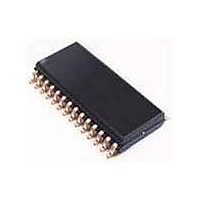
74ABT899D NXP Semiconductors, 74ABT899D Datasheet - Page 6

74ABT899D
Manufacturer Part Number
74ABT899D
Description
Bus Transceivers 9-BIT LATCH XCVR W/PARITY 3-S
Manufacturer
NXP Semiconductors
Datasheet
1.74ABT899A.pdf
(16 pages)
Specifications of 74ABT899D
Logic Type
BiCMOS
Logic Family
ABT
Number Of Channels Per Chip
8
Input Level
TTL
Output Level
TTL
Output Type
3-State
High Level Output Current
- 32 mA
Low Level Output Current
64 mA
Propagation Delay Time
4.5 ns
Supply Voltage (max)
5.5 V
Supply Voltage (min)
4.5 V
Maximum Operating Temperature
+ 85 C
Package / Case
SOP-28
Function
Latched Transceiver with Parity Checker
Minimum Operating Temperature
- 40 C
Mounting Style
SMD/SMT
Number Of Circuits
1
Polarity
Non-Inverting
Lead Free Status / Rohs Status
Details
Other names
74ABT899D,112
Available stocks
Company
Part Number
Manufacturer
Quantity
Price
Company:
Part Number:
74ABT899D
Manufacturer:
INTERSIL
Quantity:
81
1. Not more than one output should be tested at a time, and the duration of the test should not exceed one second.
2. This is the increase in supply current for each input at 3.4V.
3. For valid test results, data must not be loaded into the flip-flops (or latches) after applying the power.
4. This parameter is valid for any V
Philips Semiconductors
RECOMMENDED OPERATING CONDITIONS
DC ELECTRICAL CHARACTERISTICS
NOTES:
1998 Jan 16
SYMBOL
I
I
SYMBOL
IH
IL
9-bit dual latch transceiver with 8-bit parity
generator/checker (3-State)
I
transition time of up to 100 sec is permitted.
PU
V
I
V
I
I
I
I
T
V
V
V
OFF
+ I
+ I
CEX
CCH
CCL
CCZ
V
I
V
I
RST
I
amb
I
OH
t/ v
OH
V
OL
OL
I
/I
O
CC
CC
IK
I
IH
IL
I
PD
OZH
OZL
Input clamp voltage
High-level output voltage
Low-level output voltage
Power-up output low
voltage
Input leakage
current
Power-off leakage current
Power-up/down 3-State
output current
3-State output High current
3-State output Low current
Output High leakage current
Output current
Quiescent supply current
Additional supply current per
input pin
DC supply voltage
Input voltage
High-level input voltage
Low-level Input voltage
High-level output current
Low-level output current
Input transition rise or fall rate
Operating free-air temperature range
3
PARAMETER
2
4
1
Control pins
Data pins
CC
between 0V and 2.1V, with a transition time of up to 10msec. From V
V
V
V
V
V
V
V
V
V
V
V
V
V
V
V
V
V
V
V
V
other inputs at V
PARAMETER
CC
CC
CC
CC
CC
CC
CC
CC
CC
CC
OE
CC
CC
CC
CC
CC
CC
CC
I
CC
= GND or V
= 4.5V; I
= 4.5V; I
= 5.0V; I
= 4.5V; I
= 4.5V; I
= 5.5V; I
= 5.5V; V
= 5.5V; V
= 0.0V; V
= 2.1V; V
= Don’t care
= 5.5V; V
= 5.5V; V
= 5.5V; V
= 5.5V; V
= 5.5V; Outputs High, V
= 5.5V; Outputs Low, V
= 5.5V; Outputs 3-State;
= 5.5V; one input at 3.4V,
TEST CONDITIONS
IK
OH
OH
OH
OL
O
I
I
O
O
O
O
O
O
CC
= 1mA; V
= GND or 5.5V
= GND or 5.5V
= –18mA
or V
= 0.5V; V
= 2.7V; V
= 0.5V; V
= 5.5V; V
= 2.5V
= 64mA; V
= –3mA; V
= –3mA; V
= –32mA; V
CC
or GND
I
4.5V
I
I
I
I
I
6
= GND or V
= GND or V
= V
= V
= GND or V
I
I
I
I
= V
= V
= V
I
I
= GND or V
= V
= GND or V
IL
IL
IL
IL
IL
or V
or V
IL
or V
or V
or V
or V
IH
IH
CC
IH
IH
IH
CC
CC
IH
CC
;
CC
Min
–50
2.5
3.0
2.0
T
amb
Min
–40
4.5
2.0
0
0
–0.9
0.42
0.13
–5.0
Typ
–80
3.5
4.0
2.6
0.01
5.0
5.0
0.3
= +25 C
50
28
50
5.0
5.0
5
CC
LIMITS
LIMITS
–180
= 2.1V to V
Max
–1.2
0.55
0.55
–50
250
250
1.5
100
100
50
50
34
1.0
50
Max
V
–32
+85
5.5
0.8
T
64
5
Min
–50
CC
amb
2.5
3.0
2.0
74ABT899
to +85 C
CC
Product specification
= –40 C
= 5V
–180
Max
–1.2
0.55
0.55
–50
250
250
1.5
100
100
50
50
34
1.0
50
10%, a
UNIT
ns/V
mA
mA
V
V
V
V
C
UNIT
mA
mA
mA
V
V
V
V
V
V
A
A
A
A
A
A
A
A
A


