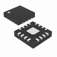
MAX4701ETE+T Maxim Integrated Products, MAX4701ETE+T Datasheet - Page 2

MAX4701ETE+T
Manufacturer Part Number
MAX4701ETE+T
Description
IC SWITCH DUAL DPDT 16TQFN
Manufacturer
Maxim Integrated Products
Datasheet
1.MAX4702EUE.pdf
(11 pages)
Specifications of MAX4701ETE+T
Function
Switch
Circuit
2 x DPDT
On-state Resistance
75 Ohm
Voltage Supply Source
Single Supply
Voltage - Supply, Single/dual (±)
1.8 V ~ 5.5 V
Current - Supply
1µA
Operating Temperature
-40°C ~ 85°C
Mounting Type
Surface Mount
Package / Case
16-TQFN Exposed Pad
Lead Free Status / RoHS Status
Lead free / RoHS Compliant
ABSOLUTE MAXIMUM RATINGS
(Voltages Referenced to GND)
V + ............................................................................-0.3V to +6V
V
Continuous Current COM_, NO_, NC_ ............................ ±20mA
ESD per Method 3015.7....................................................>2.5kV
ELECTRICAL CHARACTERISTICS—Single +3V Supply
(V+ = +2.7V to +3.3V, GND = 0, V
+85°C. Typical values are at V+ = +3V and T
Low-Voltage, Dual DPDT/Quad SPDT
Analog Switches in QFN
Peak Current COM_, NO_, NC_ (pulsed at 1ms, 10%
Note 1: Signals on IN_, COM_, NO_, and NC_ exceeding 0 or V+ are clamped by internal diodes. Limit forward-diode current to
Stresses beyond those listed under “Absolute Maximum Ratings” may cause permanent damage to the device. These are stress ratings only, and functional
operation of the device at these or any other conditions beyond those indicated in the operational sections of the specifications is not implied. Exposure to
absolute maximum rating conditions for extended periods may affect device reliability.
2
ANALOG SWITCH
L
Analog Signal Range
O n- Resi stance
O n- Resi stance M atch Betw een
C hannel s ( N ote 4)
O n- Resi stance Fl atness ( N ote 5)
N O_, N C _ O ff- Leakag e C ur r ent
( N ote 6)
COM_ On-Leakage Current
(Note 6)
DYNAMIC
Turn-On Time
Turn-Off Time
Break-Before-Make (Note 6)
On-Channel -3dB Bandwidth
Off-Isolation (Note 7)
, IN_, COM_, NO_, NC_ (Note1) .............. -0.3V to (V+ + 0.3V)
duty cycle)....................................................................±40mA
_______________________________________________________________________________________
maximum current rating.
PARAMETER
IH
V
R
I
I
SYMBOL
I
COM_ (ON)
NO_
NO_(OFF)
= +1.4V, V
NC_(OFF)
FLAT (ON)
V
ΔR
COM_
t
V
R
t
t
BBM
BW
OFF
ON
ISO
ON
, V
ON
NC_
,
A
,
= +25°C, unless otherwise noted.) (Notes 2, 3)
IL
V+ = +2.7V, I
V
V+ = +2.7V, I
V
V+ = +2.7V, I
V
+1.5V, +2V
V+ = +3.3V, V
+3V; V
V+ = +3.3V, V
+3V; V
+3V, or unconnected
V
300Ω, C
V
300Ω, C
V
300Ω, C
Signal = 0dBm, 50Ω
in and out, Figure 5
f = 1MHz, R
C
= +0.5V, (V
NO_
NO_
NO_
NO_
NO_
NO_
L
= 5pF, Figure 5
or V
or V
or V
or V
or V
or V
NO_
NO_
CONDITIONS
L
L
L
NC_
NC_
NC_
NC_
NC_
NC_
= 35pF, Figure 2
= 35pF, Figure 2
= 35pF, Figure 2
or V
or V
L
L
COM_
COM_
COM_
= 50Ω,
= +1.5V
= +1.5V
= +1V,
COM_
COM_
= +2V; R
= +2V; R
= +2V; R
= +1.5V, V
NC_
NC_
= 10mA;
= 10mA;
= 10mA;
= +3V, +1V
= +1V,
= +1V,
= +1V,
Continuous Power Dissipation (T
Operating Temperature Range .......................... -40°C to +85°C
Storage Temperature Range ........................... -65°C to +150°C
Lead Temperature (soldering, 10s) ............................... +300°C
TSSOP (derate 5.6mW/°C above +70°C) ................. 444mW
16-Pin Thin QFN (derate 20.8mW/°C
above +70°C).........................................................1666.7mW
16-Pin Thin QFN (derate 25mW/°C
above +70°C)............................................................2000mW
L
L
L
=
=
=
IH
= +1.0V, V
T
T
T
T
T
T
T
T
MIN
MIN
MIN
MIN
MIN
MIN
MIN
MIN
+25°C
+25°C
+25°C
+25°C
+25°C
+25°C
+25°C
+25°C
+25°C
T
to T
to T
to T
to T
to T
to T
to T
to T
IL
A
= +0.4V for MAX4702 only), T
MAX
MAX
MAX
MAX
MAX
MAX
MAX
MAX
MIN
-0.5
-0.5
-1
-1
0
1
A
= +70°C)
TYP
250
-76
60
27
15
15
2
8
MAX
+0.5
+0.5
V+
75
85
12
14
35
45
20
25
4
5
1
1
A
= -40°C to
UNITS
MHz
nA
nA
dB
ns
ns
ns
Ω
Ω
Ω
V


