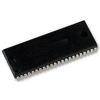
A42L0616V-50F AMIC, A42L0616V-50F Datasheet - Page 9

A42L0616V-50F
Manufacturer Part Number
A42L0616V-50F
Description
58T1323
Manufacturer
AMIC
Datasheet
1.A42L0616V-50F.pdf
(24 pages)
Specifications of A42L0616V-50F
Memory Type
DRAM
Memory Configuration
1M X 16
Access Time
50ns
Memory Case Style
TSOPII
No. Of Pins
44
Operating Temperature Range
0°C To +70°C
Ic Generic Number
42L0616
Memory Size
16Mbit
Rohs Compliant
Yes
AC Characteristics (continued)
Test Conditions:
Notes:
1.
2.
3.
4.
5.
6.
7.
8.
9.
10. t
11. t
12. These parameters are referenced to
13. Access time is determined by the longer of t
14. t
(July, 2004, Version 1.1)
47
48
49
50
51
52
53
54
#
Input timing reference level: V
Output reference level: V
Output Load: 2TTL gate + CL (50pF)
Assumed t
I
I
An initial pause of 200 µ s is required after power-up followed by any 8 RAS cycles before proper device operation is
achieved. In the case of an internal refresh counter, a minimum of 8 CAS -before- RAS initialization cycles instead of 8
AC Characteristics assume t
50pF, V
V
between V
Operation within the t
point only. If t
Operation within the t
point only. If t
Assumes three state test load (5pF and a 500 Ω Thevenin equivalent).
Either t
voltage levels.
as electrical characteristics only. If t
and data-out pins will remain open circuit, high impedance, throughout the entire cycle. If t
t
the selected cell. If neither of the above conditions is satisfied, the condition of the data out at access time is
indeterminate.
read-modify-write cycles.
RAS cycles are required. 8 initialization cycles are required after extended periods of bias without clocks.
CC1
CC1
OFF
WCS
CWD
ASC
IH
, I
(min.) and V
Symbol
, t
and I
≥ t
(max.) defines the time at which the output achieves the open circuit condition; it is not referenced to output
(min.) and t
CC3
t
t
t
t
t
t
t
t
Std
RASP
RASS
CSR
CHR
RPC
CHS
WCH
CP
OEZ
RPS
RCH
IL
, I
CC4
T
to achieve t
(min.) ≥ GND and V
=2ns
CC4
, t
IH
or t
and V
depend on output loading. Specified values are obtained with the outputs open.
RWD
RCD
RAD
, and I
RRH
Output Buffer Turn-off Delay from OE
RAS Pulse Width
RAS to CAS Precharge Time
RAS precharge time (
CAS Setup Time ( CAS -before- RAS )
CAS Hold Time
CAS hold time (
RAS pulse width (
, t
AWD
IL
is greater than the specified t
is greater than the specified t
must be satisfied for a read cycle.
IL
(max.) are reference levels for measuring timing of input signals. Transition times are measured
CWD
CC5
.
PC
≥ t
RCD
RAD
depend on cycle rate.
OH
(min.) and t
AWD
and t
/V
(max.) limit insures that t
(max.) limit insures that t
OL
IH
(min.), the cycle is a read-modify-write cycle and the data out will contain data read from
T
IH
/V
=2.0V/0.8V
AWD
= 2ns. All AC parameters are measured with a load equivalent to two TTL loads and
C
(max.) ≤ VCC.
IL
(VCC = 3.3V ± 0.3V, VSS = 0V, Ta = 0 ° C to +70 ° C or -40 ° C to +85 ° C)
=2.0V/0.8V
-B-
( CAS -before- RAS )
C
Parameter
CPA
are not restrictive operating parameters. They are included in the data sheet
(EDO Page)
-B-
R
UCAS
C
WCS
(max.) values.
self refresh)
R
-B-
self refresh)
R
≥ t
AA
self refresh)
and
RAD
RCD
or t
WCS
CAC
(max.) limit, then access time is controlled exclusively by t
(max.) limit, then access time is controlled exclusively by t
LCAS
(min.) and t
or t
RAC
RAC
CPA
leading edge in early write cycles and to WE leading edge in
(max.) can be met. t
(max.) can be met. t
8
.
WCH
Min.
100
≥ t
-50
45
10
10
76
5
-
WCH
-45
(min.), the cycle is an early write cycle
200K
Max.
2
-
-
-
-
-
-
RCD
RAD
(max.) is specified as a reference
(max.) is specified as a reference
AMIC Technology, Corp.
Min.
100
-50
50
10
10
84
5
-
A42L0616 Series
-50
RWD
200K
Max.
3
-
-
-
-
-
-
≥ t
RWD
(min.) , t
Unit
ns
ns
ns
ns
ns
µ s
ns
ns
AA
CAC
.
.
Notes
CWD
3
3
3
8
≥


