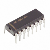
DG441DJ Maxim Integrated Products, DG441DJ Datasheet - Page 6

DG441DJ
Manufacturer Part Number
DG441DJ
Description
IC SWITCH QUAD SPST 16DIP
Manufacturer
Maxim Integrated Products
Datasheet
1.DG441DY.pdf
(9 pages)
Specifications of DG441DJ
Function
Switch
Circuit
4 x SPST - NC
On-state Resistance
85 Ohm
Voltage Supply Source
Single, Dual Supply
Voltage - Supply, Single/dual (±)
10 V ~ 30 V, ±4.5 V ~ 20 V
Operating Temperature
-40°C ~ 85°C
Mounting Type
Through Hole
Package / Case
16-DIP (0.300", 7.62mm)
Lead Free Status / RoHS Status
Contains lead / RoHS non-compliant
Available stocks
Company
Part Number
Manufacturer
Quantity
Price
Part Number:
DG441DJ
Manufacturer:
SIL
Quantity:
20 000
Company:
Part Number:
DG441DJ+
Manufacturer:
Maxim Integrated Products
Quantity:
135
Part Number:
DG441DJZ
Manufacturer:
INTERSIL
Quantity:
20 000
Using supply voltages other than ±15V reduces the
analog signal range. The DG441/DG442 switches oper-
ate with ±4.5V to ±20V bipolar supplies or with a +10V
to +30V single supply; connect V- to 0V when operating
with a single supply. Also, all device types can operate
with unbalanced supplies such as +24V and -5V. The
Typical Operating Characteristics graphs show typical
on-resistance with ±20V, ±15V, ±10V, and ±5V sup-
Improved, Quad, SPST Analog Switches
6
1, 16, 9,
DIP/SO
2, 15,
3, 14,
10, 7
11, 6
12
13
—
_______________________________________________________________________________________
8
4
5
PIN
1, 12, 9,
QFN-EP
15, 14,
16, 13,
THIN
7, 6
8, 5
10
11
—
4
2
3
Operation with Supply Voltages
Applications Information
IN1–IN4 Input
D1–D4
NAME
S1–S4
GND
N.C.
V+
EP
V-
Analog Switch Drain Terminal
Analog Switch Source
Terminal
Negative-Supply Voltage Input
Ground
Not Internally Connected
Positive-Supply Voltage
Input—Connected to Substrate
Exposed Pad. Connect EP to
V+. Do not use EP as a sole
V+ connection. (Thin QFN
package only.)
Pin Description
Other Than ±15V
FUNCTION
plies. (Switching times increase by a factor of two or
more for operation at ±5V.)
Proper power-supply sequencing is recommended for
all CMOS devices. Do not exceed the absolute maxi-
mum ratings because stresses beyond the listed rat-
ings can cause permanent damage to the devices.
Always sequence V+ on first, followed by V- and logic
inputs. If power-supply sequencing is not possible, add
two small, external signal diodes in series with supply
pins for overvoltage protection (Figure 1). Adding exter-
nal diodes reduces the analog-signal range to 1V
below V+ and 1V above V-, but low switch resistance
and low leakage characteristics are unaffected. Device
operation is unchanged, and the difference between
V+ and V- should not exceed +44V.
Figure 1. Overvoltage Protection Using External Blocking Diodes
V g
D
Overvoltage Protection
V+
V-
S


