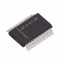
MAX4588CAI Maxim Integrated Products, MAX4588CAI Datasheet - Page 13

MAX4588CAI
Manufacturer Part Number
MAX4588CAI
Description
IC MUX DUAL RF VIDEO 4CH 28-SSOP
Manufacturer
Maxim Integrated Products
Series
4000r
Datasheet
1.MAX4588CAI.pdf
(20 pages)
Specifications of MAX4588CAI
Function
Video Multiplexer/Demultiplexer
Circuit
2 x 4:1
On-state Resistance
60 Ohm
Voltage Supply Source
Single, Dual Supply
Voltage - Supply, Single/dual (±)
2.7 V ~ 12 V, ± 2.7 V ~ 6 V
Operating Temperature
0°C ~ 70°C
Mounting Type
Surface Mount
Package / Case
28-SSOP
Lead Free Status / RoHS Status
Contains lead / RoHS non-compliant
Available stocks
Company
Part Number
Manufacturer
Quantity
Price
Part Number:
MAX4588CAI
Manufacturer:
MAXIM/美信
Quantity:
20 000
Company:
Part Number:
MAX4588CAI+
Manufacturer:
Maxim Integrated Products
Quantity:
135
Company:
Part Number:
MAX4588CAI+
Manufacturer:
MAX
Quantity:
44
The MAX4588 is constructed of high-frequency “T”
switches, as shown in Figure 8. The logic-level inputs
are translated by amplifier A1 into a V+ to V- logic sig-
nal that drives amplifier A2. Amplifier A2 drives the
gates of N-channel MOSFETs N1 and N2 from V+ to V-,
turning them fully on or off. The same signal drives
inverter A3 (which drives the P-channel MOSFETs P1
and P2, turning them fully on or off) from V+ to V-, and
turns the N-channel MOSFET N3 on and off. The logic-
level threshold is determined by V
When the switch is on, MOSFETs N1, N2, P1, and P2
are on and MOSFET N3 is off (Figure 8). The signal
path is COM_ to NO_, and because both N-channel
and P-channel MOSFETs act as pure resistances, it is
symmetrical (i.e., signals may pass in either direction).
The off MOSFET, N3, has no DC conduction, but has a
small amount of capacitance to GND. The four on
MOSFETs also have capacitance to ground that,
together with the series resistance, forms a lowpass fil-
ter. All of these capacitances are distributed evenly
along the series resistance, so they act as a transmis-
sion line rather than a simple R-C filter. The MAX4588’s
construction allows an exceptional 180MHz bandwidth
when the switches are on.
Figure 7. Serial Timing Diagram
SCLK
DOUT
DIN
CS
NOTE: ALL INPUT SIGNALS ARE SPECIFIED WITH t
TIMING IS MEASURED FROM 50% OF DIGITAL SIGNAL.
______________________________________________________________________________________
t
CSS
t
DS
Detailed Description
Logic-Level Translators
Dual 4-Channel RF/Video Multiplexer
Switch On Condition
t
t
DO
CH
A0
t
DH
L
and GND.
t
CL
R
AND t
A1
F
Low-Voltage, High-Isolation,
< 10ns.
Typical attenuation in 75Ω systems is 2.5dB and is rea-
sonably flat up to 50MHz. Higher-impedance circuits
show even lower attenuation (and vice versa), but
slightly lower bandwidth due to the increased effect of
the internal and external capacitance and the switch’s
internal resistance.
Figure 8. T-Switch Construction
COM_
INPUT
GND
V
V+
CC
V-
A2
A1
NORMALLY OPEN SWITCH CONSTRUCTION
A2
DISABLE
N1
t
CSH
A3
P1
ON GND, NO_,
ESD DIODES
AND COM_
MAX4588
N3
N2
P2
V+
V+
NO_
13


