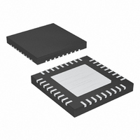
MAX4761ETX+T Maxim Integrated Products, MAX4761ETX+T Datasheet - Page 8

MAX4761ETX+T
Manufacturer Part Number
MAX4761ETX+T
Description
IC SWITCH OCTAL SPDT 36TQFN
Manufacturer
Maxim Integrated Products
Datasheet
1.MAX4760ETXT.pdf
(14 pages)
Specifications of MAX4761ETX+T
Function
Switch
Circuit
8 x SPDT
On-state Resistance
3.5 Ohm
Voltage Supply Source
Single Supply
Voltage - Supply, Single/dual (±)
1.8 V ~ 5.5 V
Current - Supply
1µA
Operating Temperature
-40°C ~ 85°C
Mounting Type
Surface Mount
Package / Case
36-WFQFN Exposed Pad
Lead Free Status / RoHS Status
Lead free / RoHS Compliant
The MAX4760/MAX4760A quad double-pole/double-
throw (DPDT) and the MAX4761/MAX4761A octal sin-
gle-pole/double-throw (SPDT) analog switches operate
from a single +1.8V to +5.5V supply. These devices are
fully specified for +3V applications.
The MAX4760/MAX4760A/MAX4761/MAX4761A have a
guaranteed 2.0Ω (typ) on-resistance to switch data or
audio signals. The low 54pF (typ) capacitance and 0.2ns
change in skew makes them ideal for data switching
applications. The MAX4760/MAX4760A have four logic
inputs to control two switches in pairs and the
MAX4761/MAX4761A have one logic control input and an
enable input (EN) to disable the switches.
The MAX4760/MAX4760A/MAX4761/MAX4761A logic
inputs accept up to +5.5V regardless of the supply volt-
age. For example, with a +3.3V supply, IN_ can be dri-
ven low to GND and high to +5.5V, which allows mixed
logic levels in a system. Driving the control logic inputs
rail-to-rail also minimizes power consumption.
For the MAX4761/MAX4761A, drive EN low to enable.
When EN is high, COM_ is high impedance.
Analog signal inputs over the full voltage range (0V to V+)
are passed through the switch with minimal change in on-
resistance (see the Typical Operating Characteristics ).
The switches are bidirectional so NO_, NC_, and COM_
can be either inputs or outputs.
Power-supply bypassing improves noise margin and
prevents switching noise from propagating from the V+
supply to other components. A 0.1µF capacitor connect-
ed from V+ to GND is adequate for most applications.
High-Bandwidth, Quad DPDT Switches
8
_______________________________________________________________________________________
Applications Information
Detailed Description
Power-Supply Bypassing
Digital Control Inputs
Analog Signal Levels
CMOS devices require proper power-supply sequenc-
ing. Always apply V+ before the analog signals, espe-
cially if the input signal is not current limited. If
sequencing is not possible, and the input signal is not
current limited to less than 20mA, add a small-signal
diode (Figure 1). Adding the diode reduces the analog
range to a diode drop (0.7V) below V+ and increases
the on-resistance slightly. The maximum supply voltage
must not exceed +6V at any time.
For the latest application details on UCSP construction,
dimensions, tape carrier information, printed circuit
board techniques, bump-pad layout, and recommend-
ed reflow temperature profile, as well as the latest infor-
mation on reliability testing results, refer to the
Application Note 1891: Wafer-Level Packaging (WLP)
and Its Applications available on Maxim’s website at
www.maxim-ic.com/ucsp.
Figure 1. Overvoltage Protection Using an External Blocking
Diode
UCSP Applications Information
NO
POSITIVE SUPPLY
Power-Supply Sequencing
V+
GND
D1
COM
MAX4760
MAX4761


