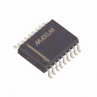
MAX382CWN+T Maxim Integrated Products, MAX382CWN+T Datasheet - Page 7

MAX382CWN+T
Manufacturer Part Number
MAX382CWN+T
Description
IC MULTIPLEXER 8X1 18SOIC
Manufacturer
Maxim Integrated Products
Series
300r
Datasheet
1.MAX382CWN.pdf
(12 pages)
Specifications of MAX382CWN+T
Function
Multiplexer
Circuit
1 x 8:1
On-state Resistance
100 Ohm
Voltage Supply Source
Single, Dual Supply
Voltage - Supply, Single/dual (±)
2.7 V ~ 16.5 V, ±3 V ~ 8 V
Operating Temperature
0°C ~ 70°C
Mounting Type
Surface Mount
Package / Case
18-SOIC (0.300", 7.50mm Width)
Lead Free Status / RoHS Status
Lead free / RoHS Compliant
The internal structures of the MAX382/MAX384 include
translators for the A2/A1/EN/WR/RS digital inputs, latch-
es, and a decode section for channel selection (see
Truth Tables ). The analog-signal switches consist of
parallel combinations of N and P MOSFETs.
WRITE (WR) and RESET (RS) strobes are provided for
interfacing with µP-bus lines, alleviating the need for the
µP to provide constant address inputs to the mux to
hold a particular channel (Figures 2–7).
When the WR strobe is in the low state (less than 0.8V)
and the RS strobe is in the high state (greater than
2.4V), the muxes are in the transparent mode—they
act similar to nonlatching devices, such as the
MAX398/MAX399.
*Analog inputs and outputs are names of convenience only. Inputs and outputs are identical and interchangeable.
______________________________________________________________Pin Description
__________Applications Information
MAX382
2, 16, 17
10–13
5–8
—
—
—
—
14
15
18
1
3
4
9
PIN
_______________________________________________________________________________________
MAX384
11–14
2, 17
9, 10
Low-Voltage, 8-Channel/Dual 4-Channel
5–8
—
—
—
—
15
16
18
1
3
4
Multiplexers with Latchable Inputs
COMA, COMB
NO1A–NO4A
NO4B–NO1B
A0, A2, A1
NO1–NO4
NO8–NO5
NAME*
A0, A1
COM
GND
WR
EN
V+
RS
V-
WRITE Logic Input
Address Logic Inputs (see Truth Tables at end of data sheet)
Address Logic Inputs (see Truth Tables at end of data sheet)
Enable Logic Input (see Truth Tables at end of data sheet)
Negative Supply Voltage Input. Connect to GND for single-supply operation.
Analog Signal Inputs—bidirectional
Analog Signal Inputs—bidirectional
Analog Signal Output—bidirectional
Analog Signal Outputs—bidirectional
Analog Signal Inputs—bidirectional
Analog Signal Inputs—bidirectional
Positive Supply Voltage Input
Ground
RESET Logic Input
When the WR goes high, the previous BCD address
input is latched and held in that state indefinitely.
RS turns off all channels when it is low. All switches stay
off until RS and EN are high and WR is low.
The MAX382/MAX384 work with both single and dual
supplies and function over the +2.4V to +16V single-
supply range. For example, with a single +5V power
supply, analog signals in the 0V to +5V range can be
switched normally. If negative signals around 0V are
expected, a negative supply is needed.
The EN latch allows all switches to be turned off under
program control. This is useful when two or more are
cascaded to build 16-line and larger analog-signal mul-
tiplexers.
FUNCTION
7


