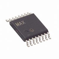
MAX14753EUE+ Maxim Integrated Products, MAX14753EUE+ Datasheet - Page 13

MAX14753EUE+
Manufacturer Part Number
MAX14753EUE+
Description
IC MULTIPLEXER DUAL 4X1 16TSSOP
Manufacturer
Maxim Integrated Products
Datasheet
1.MAX14752EUE.pdf
(15 pages)
Specifications of MAX14753EUE+
Function
Multiplexer
Circuit
2 x 4:1
On-state Resistance
130 Ohm
Voltage Supply Source
Single, Dual Supply
Voltage - Supply, Single/dual (±)
20 V ~ 72 V, ±10 V ~ 36 V
Operating Temperature
-40°C ~ 85°C
Mounting Type
Surface Mount
Package / Case
16-TSSOP
Product
Multiplexer
Number Of Lines (input / Output)
4.0 / 2.0
Supply Voltage (max)
36 V
Supply Voltage (min)
10 V
Maximum Operating Temperature
+ 85 C
Minimum Operating Temperature
- 40 C
Mounting Style
SMD/SMT
Number Of Input Lines
4.0
Number Of Output Lines
2.0
Power Dissipation
890 mW
Lead Free Status / RoHS Status
Lead free / RoHS Compliant
The MAX14752/MAX14753 are 8-to-1 and dual 4-to-1
high-voltage analog multiplexers. Both devices feature
60Ω (typ) on-resistance with 0.03Ω (typ) on-resistance
flatness. These low on-resistance multiplexers conduct
equally well in either direction.
The MAX14752 is an 8-to-1 multiplexer and MAX14753
is a dual 4-to-1 multiplexer. Both devices operate with
dual supplies of ±10V to ±36V or a single supply of
+20V to +72V. Both devices can also operate with
unbalanced supplies, such as +36V and -10V. These
multiplexers support rail-to-rail input and output signals.
The control logic level is defined via the EN input. These
devices do not require power-supply sequencing.
The current flowing through each on-channel of the
MAX14752/MAX14753 multiplexers must be limited to
±5mA for normal operation. If the current exceeds this
limit, an internal leakage current from that channel to
V
device if the max power dissipation is not exceeded.
For applications that require input voltages beyond the
normal operating voltages, the internal input diodes to
V
shown in Figure 11, series resistors can be employed at
the inputs to limit the currents flowing into the diodes dur-
ing undervoltage and overvoltage conditions. Choose the
Figure 11. Input Overvoltage and Undervoltage Clamping
SS
DD
appears. Larger input current does not destroy the
and V
SS
can be used to limit the input voltages. As
Applications Information
R
R
R
R
LIM
LIM
LIM
LIM
______________________________________________________________________________________
Detailed Description
Current Through the Mux
Input Voltage Clamping
R
LIM
R
R
R
LIM
LIM
LIM
V
V
DD
SS
8-Channel/Dual 4-Channel
72V Analog Multiplexers
limiting resistors such that the input currents are limited to
I
tors can be calculated as the larger of R
During an undervoltage or overvoltage condition, the
input impedance is equal to R
dissipation due to the fault currents needs to be calcu-
lated. The MAX14752/MAX14753 multiplexer operates
normally on a channel that is on during an overvoltage
or undervoltage clamping condition on a second chan-
nel that is not switched.
If input voltages are expected to go beyond the supply
voltages, but within the absolute maximum supply volt-
ages of the MAX14752/MAX14753, add two diodes in
series with the supplies as shown in Figure 12.
During undervoltage and overvoltage events, the internal
diodes pull V
this scheme is that the input impedance is high and
currents do not flow through the MAX14752/MAX14753
during overvoltage and undervoltage events. The input
voltages must be limited to the voltages specified in the
Absolute Maximum Ratings section.
IN_
(max) = 100mA. The values of the current limit resis-
DD
S0
R
R
/V
S1
LIM+
LIM -
CONTROL
SS
S2
supplies up/down. An advantage of
=
=
EN
V – V
V
SS
GND
IN_
I
IN_
I
IN_
Beyond-the-Rail Input
(max –V
(max
MAX14752
IN_
LIM
(max
(
)
m m in
. The additional power
)
)
DD
)
LIM+
OUT
and R
LIM-.
13


