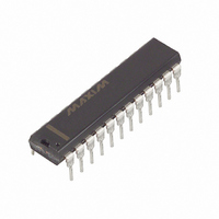
MAX335CNG+ Maxim Integrated Products, MAX335CNG+ Datasheet - Page 10

MAX335CNG+
Manufacturer Part Number
MAX335CNG+
Description
IC SWITCH OCTAL SPST 24DIP
Manufacturer
Maxim Integrated Products
Datasheet
1.MAX335CWG.pdf
(13 pages)
Specifications of MAX335CNG+
Function
Switch
Circuit
8 x SPST - NO
On-state Resistance
150 Ohm
Voltage Supply Source
Dual Supply
Voltage - Supply, Single/dual (±)
±4.5 V ~ 20 V
Operating Temperature
0°C ~ 70°C
Mounting Type
Through Hole
Package / Case
24-DIP (0.300", 7.62mm)
Number Of Switches
Octal
Switch Configuration
SPST
On Resistance (max)
150 Ohms
On Time (max)
400 ns
Off Time (max)
400 ns
Off Isolation (typ)
90 dB
Supply Voltage (max)
+/- 20 V
Supply Voltage (min)
+/- 4.5 V
Supply Current
150 uA
Maximum Power Dissipation
1067 mW
Maximum Operating Temperature
+ 70 C
Mounting Style
Through Hole
Description/function
Analog Switch
Input Level
CMOS, TTL
Minimum Operating Temperature
0 C
Off State Leakage Current (max)
1 nA
Lead Free Status / RoHS Status
Lead free / RoHS Compliant
To use the MAX335 as an 8 x 1 multiplexer, tie all
drains together (COM0 to COM7); the mux inputs now
source each switch (NO0 to NO7). Input a single 0V to
+3V pulse at DIN. As this is clocked through the regis-
ter by SCLK, each switch will sequence on one at a
time.
To use the MAX335 as a 4-2 differential multiplexer, tie
COM0 through COM3 together and COM4 through
COM7 together. Differential inputs will be the source
inputs as follows: (NO0, NO4), (NO1, NO5), (NO2,
NO6), (NO3, NO7). Figure 7 shows the serial input con-
trol at DIN required to turn on two switches making a
differential multiplexer.
CS is held low for four clock pulses; the first pulse is
clocked into the fifth switch position as the second
pulse is clocked into the first switch position. CS is
pulled high to update switches; then CS is pulled low,
and SCLK advances pulses to S1 and S5 positions,
where CS is pulled high to update, etc.
Tie COM0 to NO1 so that NO0 and COM1 are now
inputs and COM0/NO1 is the common output. SP is
common output. Up to four SPDT switches can be
made from each MAX335. Multiples of four or more can
be made by daisy chaining devices. In Figure 8, DIN is
a pulse train. Again, CS is held low to clock in pulses
and CS is pulled high to update; CS is held low to shift
pulses, then pulled high to update, etc.
Serial Controlled, 8-Channel SPST Switch
Figure 7. Differential Multiplexer Input Control
Figure 8. Serial-Input Control for SPDT Switch
10
__________Applications Information
SCLK
DIN
______________________________________________________________________________________
DIN
1 CLOCK
PULSE
4-2 Differential Multiplexer
SW4
D4
8 x 1 Multiplexer
SPDT Switches
4 CLOCK
PULSES
SWØ
DØ
Pulsing V
function. The switches are set to the off position, and
the serial shift register is reset to all zeros.
The MAX335 operates with V = ±4.5V to ±20V and
V
V+ = +10V to +30V.
The V
switching threshold. As V
threshold is raised, so the part is no longer TTL com-
patible. The MAX335 also operates with a single power
supply: V
supply cannot be used as a reset function.
TRANSISTOR COUNT: 387
SUBSTRATE CONNECTED TO V+.
COM2
___________________Chip Topography
COM0
COM1
L
NO1
NO2
GND
NO0
DIN
= +5V. With V- tied to ground, the part operates with
L
supply sets TTL input compatibility at a 1.6V
L
L
= V+ and V- = 0V. With V
V+
below +0.8V initiates the power-up reset
NO3
COM3
(2.51mm)
SCLK
0.099"
Power-Supply Operation
CS
L
COM4
is raised, the switching
NO4
VL
Reset Function
L
tied to V+, the V
NO7
COM7
NO6
DOUT
COM6
NO5
V-
COM5
(3.96mm)
0.156"
L


