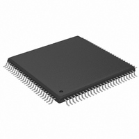
MAX9675ECQ+ Maxim Integrated Products, MAX9675ECQ+ Datasheet - Page 6

MAX9675ECQ+
Manufacturer Part Number
MAX9675ECQ+
Description
IC CROSSPOINT SWIT 16X16 100TQFP
Manufacturer
Maxim Integrated Products
Datasheet
1.MAX9675ECQT.pdf
(27 pages)
Specifications of MAX9675ECQ+
Function
Crosspoint Switch
Circuit
1 x 16:16
Voltage Supply Source
Single Supply
Voltage - Supply, Single/dual (±)
2.7 V ~ 5.5 V
Operating Temperature
-40°C ~ 85°C
Mounting Type
Surface Mount
Package / Case
100-TQFP Exposed Pad
Lead Free Status / RoHS Status
Lead free / RoHS Compliant
110MHz, 16 x 16 Video Crosspoint
Switch with Programmable Gain
SWITCHING CHARACTERISTICS
(V
= +1V/V, and T
Note 1: Associated output voltage may be determined by multiplying the input voltage by the specified gain (A
Note 2: Logic-level characteristics apply to the following pins: DIN, DOUT, SCLK, CE, UPDATE, RESET, A3–A0, MODE, and AOUT.
Note 3: Switching transient settling time is guaranteed by the settling time (t
Note 4: Input test signal: 3.58MHz sine wave of amplitude 40IRE superimposed on a linear ramp (0 to 100IRE). IRE is a unit of
Note 5: All devices are 100% production tested at T
6
Delay: UPDATE to Video Out
Delay: UPDATE to AOUT
Delay: SCLK to DOUT Valid
Delay: Output Disable
Delay: Output Enable
Setup: CE to SCLK
Setup: DIN to SCLK
Hold Time: SCLK to DIN
Minimum High Time: SCLK
Minimum Low Time: SCLK
Minimum Low Time: UPDATE
Setup Time: UPDATE to SCLK
Hold Time: SCLK to UPDATE
Setup Time: MODE to SCLK
Hold Time: MODE to SCLK
Minimum Low Time: RESET
Delay: RESET
CC
_______________________________________________________________________________________
= +5V, V
offset voltage.
ing the switch matrix.
video-signal amplitude developed by the International Radio Engineers: 140IRE = 1.0V.
PARAMETER
EE
A
= T
= -5V, V
MIN
to T
DD
MAX
= +2.7V to +5.5V, DGND = AGND = 0, V
, unless otherwise noted. Typical values are at T
SYMBOL
t
t
t
t
t
t
t
t
PdUdVo
PdUdAo
t
t
HdHUd
t
MnLRst
t
PdHOe
MnHCk
MnLUd
SuHUd
t
t
PdLOe
t
MnLCk
t
PdDo
t
HdMd
PdRst
SuMd
SuCe
HdDi
SuDi
V
MODE = 0, time to AOUT = low after
UPDATE = low
V
Output disabled, 1kΩ pulldown to AGND,
V
Rising edge of UPDATE to falling edge of
SCLK
Falling edge of SCLK to falling edge of
UPDATE
Minimum time from clock edge to MODE
with valid data clocking
Minimum time from clock edge to MODE
with valid data clocking
10kΩ pulldown to AGND, 0.5V step
Logic state change in DOUT on active
SCLK edge
IN_
OUT_
IN_
A
= 0.5V step
= 0.5V
= +25°C. Specifications over temperature limits are guaranteed by design.
= 0.5V, 1kΩ pulldown to AGND
CONDITIONS
IN
_ = 0 for dual supplies, R
S
) specification. Switching transient is a result of updat-
A
= +25°C.) (Note 5)
L
MIN
= 150Ω to AGND, C
100
100
100
100
100
100
100
100
100
TYP
200
300
200
30
30
V
) and adding output
MAX
200
450
200
800
100
300
600
800
L
= 100pF, A
UNITS
ns
ns
ns
ns
ns
ns
ns
ns
ns
ns
ns
ns
ns
ns
ns
ns
ns
V


