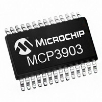
MCP3903-I/SS Microchip Technology, MCP3903-I/SS Datasheet - Page 3

MCP3903-I/SS
Manufacturer Part Number
MCP3903-I/SS
Description
IC AFE 24BIT 64KSPS 28SSOP
Manufacturer
Microchip Technology
Series
-r
Datasheet
1.MCP3903-ISS.pdf
(54 pages)
Specifications of MCP3903-I/SS
Featured Product
MCP3903 Six Channel ÎΣ A/D Converter
Number Of Bits
24
Number Of Channels
6
Power (watts)
-
Voltage - Supply, Analog
4.5 V ~ 5.5 V
Voltage - Supply, Digital
2.7 V ~ 3.6 V
Package / Case
28-SSOP (0.209", 5.30mm Width)
Lead Free Status / Rohs Status
Lead free / RoHS Compliant
Available stocks
Company
Part Number
Manufacturer
Quantity
Price
Company:
Part Number:
MCP3903-I/SS
Manufacturer:
Microchip
Quantity:
263
Part Number:
MCP3903-I/SS
Manufacturer:
MICROCHIP/微芯
Quantity:
20 000
1.0
The Reliability Targets section includes the absolute
maximum ratings for the device, defining the values
that will cause no long term damage regardless of
duration.
These tables also represent the testing requirements
per the Max. and Min. columns.
TABLE 1-1:
© 2011 Microchip Technology Inc.
Electrical Specifications: Unless otherwise indicated, all parameters apply at AV
3.6V, Internal V
GAIN = 1, V
Internal Voltage Reference
A001
A002
A003
Voltage Reference Input
A004
A005
A006
A007
ADC Performance
A008
A009
A010
Note 1:
Param.
Num.
2: See terminology section for definition.
3: This parameter is established by characterization and not 100% tested.
4: For these operating currents, the following configuration bit settings apply: Config Register Settings:
5: For these operating currents, the following configuration bit settings apply: Config Register Settings:
6: Applies to all gains. Offset error is dependant on PGA gain setting.
7: Outside of this range, ADC accuracy is not specified. An extended input range of +/- 6V can be applied continuously to
8: For proper operation and to keep ADC accuracy, AMCLK should always be in the range of 1 to 5 MHz with BOOST bits
CHARACTERISTICS
ELECTRICAL
instability across this input range. Dynamic Performance is specified at -0.5 dB below the maximum signal range,
V
SHUTDOWN<5:0> = 000000, RESET<5:0> = 000000; VREFEXT = 0, CLKEXT = 0.
SHUTDOWN<5:0> = 111111, VREFEXT = 1, CLKEXT = 1.
the part with no risk for damage.
off. With BOOST bits on, AMCLK should be in the range of 1 to 8.192 MHz. AMCLK = MCLK/PRESCALE. When using a
crystal, CLKEXT bit should be equal to ‘0’.
This specification implies that the ADC output is valid over this entire differential range, i.e. there is no distortion or
IN
ZOUT
IN
Symbol
= -0.5 dBFS @ 50/60 Hz = 333 mV
TC
V
V
V
V
= 1V
REF+
REF-
REF
REF
REF
f
f
REF
S
D
ANALOG SPECIFICATIONS TARGET TABLE
REF
, MCLK = 4 MHz;PRESCALE = 1; OSR = 64; f
PP
= 353mV
Voltage
Tempco
Output Impedance
Input Capacitance
Differential Input Voltage
Range (V
Absolute Voltage on REFIN+
pin
Absolute Voltage on REFIN-
pin
Resolution (No Missing
Codes)
Sampling Frequency
Output Data Rate
Characteristic
RMS
REF+
@ 50/60 Hz.
- V
REF-
RMS
)
, V
REF
= 2.4V.
Min.
-2%
-0.3
2.2
1.9
—
—
See
See
Typ.
2.35
1.1
ABSOLUTE MAXIMUM RATINGS †
V
Digital inputs and outputs w.r.t. A
Analog input w.r.t. A
V
Storage temperature ..................................... -65°C to +150°C
Ambient temp. with power applied................ -65°C to +125°C
Soldering temperature of leads (10 seconds)............. +300°C
ESD on the analog inputs (HBM,MM)................. 5.0 kV, 500V
ESD on all other pins (HBM,MM)........................ 5.0 kV, 500V
24
—
—
—
—
Table 4-2
Table 4-2
5
7
DD
REF
S
................................................................................... 7.0V
= 1 MHz; f
input w.r.t. A
Max.
+2%
+0.3
2.6
2.9
—
—
10
RELIABILITY TARGETS
D
= 15.625 ksps; T
ppm/°C VREFEXT = 0
GND
Units
ksps
kHz
bits
GND
kΩ
pF
V
V
V
V
DD
................................-0.6V to V
..................................... ....-6V to +6V
= 4.5 to 5.5V, DV
VREFEXT = 0
AV
VREFEXT = 0
V
VREFEXT = 1
VREFEXT = 1
V
to AGND when VREFEXT=0
OSR = 256 (see
f
PRESCALE)
f
= MCLK / (4 x PRESCALE x
OSR)
S
D
REF
REF-
= DMCLK = MCLK / (4 x
= DRCLK= DMCLK / OSR
DD
GND
MCP3903
=5V,
= (V
Test Conditions
should be connected
A
........-0.6V to V
= -40°C to +125°C,
REF+
DS25048B-page 3
DD
- V
Table
= 2.7 to
REF-
DD
DD
),
5-2)
+0.6V
+0.6V


