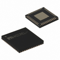
SY89540UMI Micrel Inc, SY89540UMI Datasheet
SY89540UMI
Specifications of SY89540UMI


Related parts for SY89540UMI


SY89540UMI Summary of contents
Page 1
General Description The SY89540U is a low-jitter, low skew, high-speed 4x4 crosspoint switch optimized for precision telecom and enterprise server/storage distribution applications. The SY89540U guarantees data-rates up to 3.2Gbps over temperature and voltage. The SY89540U differential input includes Micrel’s unique, ...
Page 2
Functional Block Diagram December 2007 2 hbwhelp@micrel.com M9999-120607-C or (408) 955-1690 ...
Page 3
... Ordering Information Part Number SY89540UMI (2) SY89540UMITR SY89540UMY (2) SY89540UMYTR Notes: 1. Contact factory for die availability. Dice are guaranteed Tape and Reel ordering option. Pin Configuration December 2007 Package Temperature Type Range QFN-44 Industrial QFN-44 Industrial QFN-44 Industrial QFN-44 Industrial = 25°C, DC electrical only. ...
Page 4
Pin Description Pin Number Pin Name 17, 15, IN0, /IN0, 10, 8 IN1, /IN1 IN2, /IN2, 41, 39 IN3, /IN3 16, 9, VT0, VT1 VT2, VT3 14, VREF_AC0, 11, VREF_AC1, 1, VREF_AC2, 42 VREF_AC3 18, 19 ...
Page 5
Functional Description Buffer Mode SY89540 can be used as a 1:4 fanout buffer. This is the default mode with LOAD and CONFIG being HIGH when the device is first powered up. The SIN0 and SIN1 inputs select the input signal ...
Page 6
Absolute Maximum Ratings Supply Voltage (V ) ..........................–0.5V to +4.0V CC Input Voltage (V ) ..................................–0. CML Output Voltage (V ) .... V OUT (3) Termination Current Source or sink current Input Current Source ...
Page 7
LVDS Outputs DC Electrical Characteristics V = 2.5V ±5 –40°C to +85° Symbol Parameter V Output HIGH Voltage OH (Q, /Q) V Output LOW Voltage OL (Q, /Q) V Output Voltage Swing OUT (Q, /Q) ...
Page 8
AC Electrical Characteristics V = 2.5V ±5 –40°C to +85° Symbol Parameter f Maximum Operating Frequency MAX t Propagation Delay Tempco Set-up Time t S SIN-to-LOAD SOUT-to-LOAD LOAD-to-CONFIG CONFIG-to-LOAD t Hold Time ...
Page 9
Single-Ended and Differential Swing Figure 1a. Single-Ended Voltage Swing Timing Diagram Truth Tables Input Select Address Table SIN1 SIN0 December 2007 Figure 1b. Differential Voltage Swing Figure 2. Timing Diagram Input SOUT1 ...
Page 10
Typical Operating Characteristics 100mV, at 25° Amplitude vs. Frequency 350 300 250 200 150 100 50 FREQUENCY (MHz) Channel-to-Channel Skew, Relative to Ch0 ...
Page 11
Functional Characteristics 100mV, at 25° Clock Pattern Data Pattern December 2007 11 hbwhelp@micrel.com M9999-120607-C or (408) 955-1690 ...
Page 12
Input and Output Stage Internal Termination Figure 3. Simplified Differential Input Stage December 2007 Output Stage Internal Termination On a nominal 1.25V common mode above ground, LVDS specifies a small swing of 350mV, typical. The common mode voltage has tight ...
Page 13
Input Interface Applications Figure 5a. LVPECL Interface (DC-Coupled) Figure 5d. CML Interface (AC-Coupled) Related Product and Support Documentation Part Number Function SY58540U Ultra Precision 4x4 CML Crosspoint Switch w/Internal I/O Termination HBW Solutions New Products and Applications December 2007 Figure ...
Page 14
Package Information MICREL, INC. 2180 FORTUNE DRIVE SAN JOSE, CA 95131 USA TEL +1 (408) 944-0800 FAX +1 (408) 474-1000 WEB http:/www.micrel.com The information furnished by Micrel in this data sheet is believed to be accurate and reliable. However, no ...