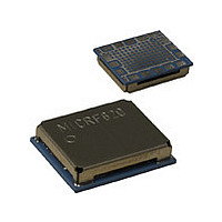
MICRF620 Micrel Inc, MICRF620 Datasheet - Page 16

MICRF620
Manufacturer Part Number
MICRF620
Description
Manufacturer
Micrel Inc
Datasheet
1.MICRF620.pdf
(21 pages)
Specifications of MICRF620
Operating Temperature (min)
-20C
Operating Temperature Classification
Commercial
Modulation Type
FSK
Lead Free Status / Rohs Status
Not Compliant
RSSI
A Typical plot of the RSSI voltage as function of input
power is shown in Figure 10. The RSSI has a dynamic
range of about 50dB from about -110dBm to -60dBm input
power.
The RSSI can be used as a signal presence indicator.
When a RF signal is received, the RSSI output increases.
This could be used to wake up circuitry that is normally in
a sleep mode configuration to conserve battery life.
Another application for which the RSSI could be used is to
determine if transmit power can be reduced in a system. If
the RSSI detects a strong signal, it could tell the
transmitter to reduce the transmit power to reduce current
consumption.
FEE
The Frequency Error Estimator (FEE) uses information
from the demodulator to calculate the frequency offset
between the receive frequency and the transmitter
frequency. The output of the FEE can be used to tune the
XCO frequency, both for production calibration and for
compensation for crystal temperature drift and aging.
The input to the FEE circuit are the up and down pulses
from the demodulator. Every time a ‘1’ is updated, an UP-
pulse is coming out of the demodulator and the same with
the DN-pulse every time the ‘0’ is updated. The expected
no. of pulses for every received symbol is 2 times the
modulation index (∆).
Micrel, Inc.
July 2006
0010101
0010110
A6..A0
0000001
A6..A0
2,25
1,75
1,25
0,75
1,5
0,5
2
1
-120
FEE_7
D7
-
D7
‘1’
-110
FEE_6
D6
D6
-
‘0’
33kohm, 1nF, 20kbps, BW=200kHz, Vdd=2.5V
Figure 10. RSSI Voltage
D5
‘0’
FEE_5
-100
D5
-
D4
‘0’
Input power [dBm]
FEE_4
D4
RSSI
-90
-
RSSI_en
D3
FEEC_3
FEE_3
D3
-80
LD_en
D2
FEEC_2
FEE_2
D2
-70
PF_FC1
D1
FEEC_1
FEE_1
D1
-60
PF_FC0
D0
FEEC_0
FEE_0
D0
-50
16
The FEE can operate in three different modes; counting
only UP-pulses, only DN-pulses or counting UP+DN
pulses. The no. of received symbols to be counted is either
8, 16, 32 or 64. This is set by the FEEC_0…FEEC_3
control bit, as follows:
The result of the measurement is the FEE value, this can
be read from register with address 0010110b. Negative
values are stored as a binary no between 0000000 and
1111111. To calculate the negative value, a two’s
complement of this value must be performed. Only FEE
modes where DN-pulses are counted (10 and 11) will give
a negative value.
When the FEE value has been read, the frequency offset
can be calculated as follows:
where FEE is the value stored in the FEE register, (Fp is
the single sided frequency deviation, P is the no. of
symbols/data bit counted and R is the symbol/data rate. A
positive Foffset means that the received signal has a
higher frequency than the receiver frequency. To
compensate for this, the receivers XCO frequency should
be increased.
It is recommended to use Mode UP+DN for two reasons,
you do not need to know the actual frequency deviation
and this mode gives the best accuracy.
FEEC_1
FEEC_3
Mode UP:
Mode DN:
Mode UP+DN: Foffset = R/(4P)x(FEE)
0
0
1
1
0
0
1
1
FEEC_0
FEEC_2
0
1
0
1
0
1
0
1
Table 8. FEEC Control Bit
Foffset = R/(2P)x(FEE-∆Fp)
Foffset = R/(2P)x(FEE+∆Fp)
FEE Mode
Off
Counting UP pulses
Counting DN pulses
Counting UP and DN pulses. UP
increments the counter, DN
decrements it.
No. of symbols used for the
measurement
8
16
32
65
MICRF620/MICRF620Z
M9999-120205


