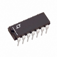
LT1684CN#PBF Linear Technology, LT1684CN#PBF Datasheet - Page 5

LT1684CN#PBF
Manufacturer Part Number
LT1684CN#PBF
Description
IC RING TONE GENERATOR 14-DIP
Manufacturer
Linear Technology
Datasheet
1.LT1684CN.pdf
(16 pages)
Specifications of LT1684CN#PBF
Function
Tone Generator
Number Of Circuits
1
Operating Temperature
0°C ~ 125°C
Mounting Type
Through Hole
Package / Case
14-DIP (0.300", 7.62mm)
Lead Free Status / RoHS Status
Lead free / RoHS Compliant
Current - Supply
-
Voltage - Supply
-
Power (watts)
-
Interface
-
Available stocks
Company
Part Number
Manufacturer
Quantity
Price
PI FU CTIO S
IN B (Pin 1): PWM Negative Input. Input is isolated from
digital source by ~100pF series capacitor. A 10k resistor
can be connected to the IN B pin in series with the isolation
capacitor for transient protection. The PWM receiver imple-
ments a diode forward drop of input hysteresis (relative to
IN A). This hysteresis and internal signal limiting assure
common mode glitch rejection with isolation capacitor
mismatches up to 2:1. For maximum performance, how-
ever, effort should be made to match the two PWM input
isolation capacitors. Pin IN B is differentially clamped to
pin IN A through back-to-back diodes. This results in a
high impedance differential input through 100mV be-
yond the input thresholds. 5k internal input resistors yield
a 10k (nominal) differential overdrive impedance.
COMP1 (Pin 2): Output Amplifier Primary Compensation.
Connect a 100pF capacitor from pin COMP1 to pin OUT.
COMP2 (Pin 3): Output Amplifier Secondary Compensa-
tion. Connect a 20pF capacitor from pin COMP2 to pin
OUT.
LIM
implements I
resistor has a typical value of 3.5 . For maximum current
drive capability (190mA typical) short pin to pin V
Reduction of current sink capability is achieved by placing
additional resistance from pin LIM
external 3.5
reduce the current sinking capability of the output ampli-
fier by approximately 50%.)
V
the source of the active tracking supply P-channel MOSFET.
V
V
AT
GATE
sources current from pull-down resistor to bias gate of
active tracking supply P-channel MOSFET. Self-biases to
a typical value of –14V, referenced to pin AT
resistor value is determined such that current sourced
from the GATE
mum output signal voltage and less than 10mA at maxi-
mum output signal voltage.
GS
–
–
REF
U
rail voltage is GATE
(Pin 5): Local Negative Supply. Typically connected to
. Typical P-channel MOSFET characteristics provide
–
–
(Pin 4): Output Amplifier Current Sink Limit. Pin
– V
(Pin 6): Negative Power Supply FET Gate Drive. Pin
U
–
OUT
10V.
resistance from pin LIM
–
pin remains greater than 50 A at mini-
• R = V
U
–
self-bias voltage less the MOSFET
BE
current clamp. Internal clamp
–
to pin V
–
REF
to pin V
. Pull-down
–
. (i.e. An
–
will
–
.
AT
cally connected to pin OUT. Pin bias current is the differ-
ence between the magnitudes of GATE
GATE
OUT (Pin 8): Ring Tone Output Pin. Output of active filter
amplifier/buffer. Used as reference voltage for internal
functions of IC. Usually shorted to pin AT
reference for active tracking supply circuitry. Connect a 1A
(1N4001-type) diode between V
1A Schottky diode from V
protection.
LIM
implements I
resistor has a typical value of 3.5 . For maximum current
drive capability (190mA typical) short pin LIM
OUT. Reduction of current source capability is achieved by
placing additional resistance from pin LIM
(i.e. An external 3.5 resistance from pin LIM
will reduce the current sourcing capability of the output
amplifier by approximately 50%.)
V
the source of the active tracking supply N-channel MOSFET.
This condition should be made using a ferrite bead.
Operating V
the MOSFET V
tics provide V
GATE
Pin sinks current from pull-up resistor to bias gate of
active tracking supply N-channel MOSFET. Self-biases to
a typical value of 14V, referenced to pin AT
resistor value is determined such that sink current into
GATE
signal voltage and less than 10mA at minimum output
signal voltage.
AMPIN (Pin 12): Output Amplifier Input. Connected to
external filter components through series protection re-
sistor (usually 5k). Thevenin DC resistance of external
filter and protection components should be 10k for opti-
mum amplifier offset performance. See Applications In-
formation section.
+
REF
(Pin 10): Local Positive Supply. Typically connected to
+
–
(Pin 9): Output Amplifier Current Source Limit. Pin
+
+
(Pin 7): Active Tracking Supply Reference. Typi-
pin bias (I
pin remains greater than 50 A at maximum output
(Pin 11): Positive Power Supply FET Gate Drive.
+
OUT
rail voltage is GATE
GS
+
– AT
. Typical N-channel MOSFET characteris-
ATREF
• R = V
REF
= I
BE
10V.
current clamp. Internal clamp
GATE
–
to OUT for line transient
+ – I
+
self-bias voltage less
+
and OUT and a
GATE
+
REF
LT1684
+
pin bias and
– ).
REF
+
to pin OUT.
to generate
to pin OUT
. Pull-up
+
to pin
5


