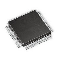
SI3225-KQ Silicon Laboratories Inc, SI3225-KQ Datasheet - Page 9

SI3225-KQ
Manufacturer Part Number
SI3225-KQ
Description
IC SLIC/CODEC DUAL-CH 64TQFP
Manufacturer
Silicon Laboratories Inc
Series
ProSLIC®r
Specifications of SI3225-KQ
Package / Case
*
Function
Subscriber Line Interface Concept (SLIC), CODEC
Interface
GCI, PCM, SPI
Number Of Circuits
2
Voltage - Supply
3.3V, 5V
Current - Supply
65mA
Power (watts)
941mW
Operating Temperature
0°C ~ 70°C
Mounting Type
Surface Mount
Includes
Battery Switching, BORSCHT Functions, DTMF Generation and Decoding, FSK Tone Generation, Modem and Fax Tone Detection
Product
SLIC
Supply Voltage (min)
3.13 V
Supply Current
22 mA
Maximum Operating Temperature
+ 70 C
Minimum Operating Temperature
0 C
Mounting Style
SMD/SMT
Number Of Channels
2
Lead Free Status / RoHS Status
Contains lead / RoHS non-compliant
Available stocks
Company
Part Number
Manufacturer
Quantity
Price
Company:
Part Number:
SI3225-KQ
Manufacturer:
Silicon Laboratories Inc
Quantity:
10 000
Table 5. AC Characteristics
(V
Parameter
Overload Level
Overload Compression
Single Frequency Distortion
Signal-to-(Noise + Distortion)
Ratio
Audio Tone Generator Signal-to-
Distortion Ratio
Intermodulation Distortion
Gain Accuracy
Attenuation Distortion vs. Freq.
Group Delay vs. Frequency
Gain Tracking
Round-Trip Group Delay
Crosstalk between channels
TX or RX to TX
TX or RX to RX
Gain Step Increment
2-Wire Return Loss
Notes:
DD
1. The input signal level should be 0 dBm0 for frequencies greater than 100 Hz. For 100 Hz and below, the level should
2. Analog signal measured as V
3. The quantization errors inherent in the µ/A-law companding process can generate slightly worse gain tracking
4. The digital gain block is a linear multiplier that is programmable from –∞ to +6 dB. The step size in dB varies over the
5. V
6. The level of any unwanted tones within the bandwidth of 0 to 4 kHz does not exceed –55 dBm.
7. The OBIAS and ABIAS registers program the dc bias current through the SLIC in the on-hook transmission and off-
, V
2
DD1
be –10 dBm0. The output signal magnitude at any other frequency will be smaller than the maximum value specified.
performance in the signal range of 3 to –37 dB for signal frequencies that are integer divisors of the 8 kHz PCM
sampling rate.
complete range. See “Audio Path Processing”.
hook active conditions, respectively. This per-pin total current setting should be selected so it can accommodate the
sum of the metallic and longitudinal currents through each of the TIP and RING leads for a given application.
DD1
–V
–V
DD4
DD4
3
2
2
= 3.13 to 5.25 V, T
= 3.3 V, V
5
4
BAT
1
= –52 V, no fuse resistors, R
A
TIP
= 0 to 70 °C for K-Grade, –40 to 85 °C for B-Grade)
– V
Active off-hook, and OHT, any Z
2-Wire to PCM or PCM to 2-Wire
2-Wire – PCM or PCM – 2-Wire:
1014 Hz, Within same time-slot
0 dBm0, Active off-hook, and
RING
V
1014 Hz, Any gain setting
V
reference level –10 dBm
DD1
PCM – 2-Wire – PCM:
Step size around 0 dB
DD1
. Assumes ideal line impedance matching.
1014 Hz sine wave,
16-bit Linear mode
200 Hz to 3.4 kHz
200 Hz – 3.4 kHz,
200 Hz to 3.4 kHz
300 Hz to 3.4 kHz
300 Hz to 3.4 kHz
200 Hz to 3.4 kHz
–37 dB to –50 dB
–50 dB to –60 dB
D/A or A/D 8-bit
Test Condition
TX/RX Performance
3 dB to –37 dB
– V
Preliminary Rev. 0.91
2-Wire – PCM
– V
OHT, any Z
Signal level:
0 dBm 0
0 dBm0,
DD4
DD4
= 3.3 V ± 5%
= 5 V ± 5%
L
= 600 Ω, Z
T
S
= 600 Ω synthesized using RS register coefficients.
T
Figure 7,8
Figure 6
Figure 5
Figure 9
–0.25
–0.1
Min
2.5
46
26
—
—
—
—
—
—
—
—
—
—
—
Si3220/Si3225
±0.0005
Typ
450
30
—
—
—
—
—
—
—
—
—
—
—
—
—
—
—
—
—
± 0.25
+0.25
+ 0.4
± 0.5
± 1.0
Max
–65
–65
–41
500
–75
–75
—
—
—
—
—
—
—
—
—
Unit
V
dB
dB
dB
dB
dB
dB
dB
dB
dB
dB
dB
dB
dB
µs
—
—
—
PK
9


