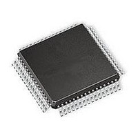
SI3220-GQ Silicon Laboratories Inc, SI3220-GQ Datasheet - Page 66

SI3220-GQ
Manufacturer Part Number
SI3220-GQ
Description
IC SLIC/CODEC DUAL-CH 64TQFP
Manufacturer
Silicon Laboratories Inc
Series
ProSLIC®r
Specifications of SI3220-GQ
Function
Subscriber Line Interface Concept (SLIC), CODEC
Interface
GCI, PCM, SPI
Number Of Circuits
2
Voltage - Supply
3.3V, 5V
Current - Supply
65mA
Power (watts)
941mW
Operating Temperature
-40°C ~ 85°C
Mounting Type
Surface Mount
Package / Case
*
Includes
Battery Switching, BORSCHT Functions, DTMF Generation and Decoding, FSK Tone Generation, Modem and Fax Tone Detection
Lead Free Status / RoHS Status
Lead free / RoHS Compliant
Available stocks
Company
Part Number
Manufacturer
Quantity
Price
Company:
Part Number:
SI3220-GQ
Manufacturer:
Silicon Laboratories Inc
Quantity:
10 000
Part Number:
SI3220-GQ
Manufacturer:
SILICONLABS/芯科
Quantity:
20 000
Company:
Part Number:
SI3220-GQR
Manufacturer:
SILICON
Quantity:
15 000
Si3220/Si3225
Table 39 outlines the hex codes corresponding to the
detected DTMF digits.
Modem Tone Detection
The Dual ProSLIC devices are capable of detecting a
2100 Hz
Recommendation V.8. The detection scheme can be
implemented in both transmit and receive paths and is
enabled by programming the appropriate register bit.
The detection scheme should be disabled for power
conservation after the modem tone window has passed.
Once a valid modem tone is detected, a register bit is
set accordingly, and the user can check the results by
reading the register value. A programmable debounce
interval is provided to eliminate false detection and can
be programmed in increments of 67 ms by writing to the
appropriate register.
Audio Path Processing
Unlike traditional SLICs, the Dual ProSLIC devices
integrate the codec function into the same IC. The on-
chip 16-bit codec offers programmable gain/attenuation
blocks and multiple loopback modes for self testing. The
signal path block diagram is shown in Figure 11 on page
24.
66
modem
Table 39. DTMF Hex Codes
Digit
C
D
A
B
1
2
3
4
5
6
7
8
9
0
#
*
tone
as
Hex code
0xC
0xD
0xA
0xB
0xE
0xF
described
0x1
0x2
0x3
0x4
0x5
0x6
0x7
0x8
0x9
0x0
in
ITU-T
Rev. 1.0
Transmit Path
In the transmit path, the analog signal fed by the
external ac coupling capacitors is passed through an
anti-aliasing filter before being processed by the A/D
converter. An analog mute function is provided directly
prior to the A/D converter input. The output of the A/D
converter is an 8 kHz, 16-bit wide, linear PCM data
stream. The standard requirements for transmit path
attenuation for signals above 3.4 kHz are part of the
combined decimation filter characteristic of the A/D
converter. One more digital filter, THPF, is available in
the transmit path. THPF implements the high-pass
attenuation requirements for signals below 65 Hz. An
equalizer block then equalizes the transmit signal path
to compensate for series protection resistance, R
outside of the ac-sensing inputs. The linear PCM data
stream output from the equalizer block is amplified by
the transmit-path programmable gain amplifier, TPGA,
which can be programmed from –
decoder receives the linear PCM data stream and
performs the digit extraction if enabled by the user. The
final step in the transmit path signal processing is the
A-law or µ -law compression, which can reduce the data
stream word width to 8 bits. Depending on the PCM
mode select register selection, every 8-bit compressed
serial data word occupies one time slot on the PCM
highway, or every 16-bit uncompressed serial data
word occupies two time slots on the PCM highway.
Receive Path
In the receive path, the optionally-compressed 8-bit
data is first expanded to 16-bit words. The PCMF
register bit can bypass the expansion process so that
two 8-bit words are assembled into one 16-bit word.
RPGA is the receive path programmable gain amplifier,
which can be programmed from – ∞ dB to 6 dB. An
8 kHz, 16-bit signal is then provided to a D/A converter.
An analog mute function is provided directly after the
D/A converter. When not muted, the resulting analog
signal is applied at the input of the transconductance
amplifier, Gm, which drives the off-chip current buffer,
I
TPGA/RPGA Gain/Attenuation Blocks
The TPGA and RPGA blocks are essentially linear
multipliers with the structure illustrated in Figure 39.
Both blocks can be independently programmed from –
to +6 dB (0 to 2 linear scale). The TXGAIN and RXGAIN
RAM locations are used to program each block. A
setting of 0000h mutes all audio signals; a setting of
4000h passes the audio signal with no gain or
attenuation (0 dB), and a setting of 7FFFh provides the
maximum 6 dB of gain to the incoming audio signal. The
DTXMUTE and DRXMUTE bits in the DIGCON register
BUF
.
∞
to 6 dB. The DTMF
PROT
∞
,


