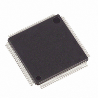
DS21Q50L+ Maxim Integrated Products, DS21Q50L+ Datasheet - Page 56

DS21Q50L+
Manufacturer Part Number
DS21Q50L+
Description
IC TXRX E1 QUAD 100-LQFP
Manufacturer
Maxim Integrated Products
Datasheet
1.DS21Q50L.pdf
(87 pages)
Specifications of DS21Q50L+
Function
Transceiver
Interface
E1
Number Of Circuits
4
Voltage - Supply
3.14 V ~ 3.47 V
Current - Supply
230mA
Operating Temperature
0°C ~ 70°C
Mounting Type
Surface Mount
Package / Case
*
Includes
AIS Alarms Detector and Generator, Loopback Functions, PRBS Generator / Detector, Remote Detector and Generator
Lead Free Status / RoHS Status
Lead free / RoHS Compliant
Power (watts)
-
16.
The line interface unit in the DS21Q50 contains three sections: the receiver, which handles clock and data
recovery; the transmitter, which waveshapes and drives the E1 line; and the jitter attenuator. The line
interface control register (LICR), described below, controls each of these three sections.
Register Name:
Register Description:
Register Address:
Bit
Name
16.1 Receive Clock and Data Recovery
The DS21Q50 contains a digital clock-recovery system. See
The device couples to the receive E1 shielded twisted pair or coax through a 1:1 transformer
(Table
internal PLL and fed to the clock recovery system. The clock recovery system uses the clock from the
PLL circuit to form a 16 times oversampler, which is used to recover the clock and data. This over-
sampling technique offers outstanding jitter tolerance
Normally, RCLK is the recovered clock from the E1 AMI/HDB3 waveform presented at the RTIP and
RRING inputs. When no AMI signal is present at RTIP and RRING, a receive carrier loss (RCL)
condition occurs, and the RCLK is sourced from the clock applied at the MCLK pin. If the jitter
attenuator is either placed in the transmit path or is disabled, RCLK can exhibit slightly shorter high
cycles of the clock. This is because of the highly oversampled digital clock-recovery circuitry. If the jitter
attenuator is placed in the receive path (as is the case in most applications), the jitter attenuator restores
the RCLK to being close to 50% duty cycle. See the Receive AC Characteristics in Section
details.
NAME
JABDS
EGL
TPD
DJA
JAS
L2
L1
L0
16-4). The 2.048MHz clock attached at the MCLK pin is internally multiplied by 16 through an
LINE INTERFACE UNIT
L2
7
BIT
7
6
5
4
3
2
1
0
Line Build-Out Select Bit 2. Sets the transmitter build-out.
Line Build-Out Select Bit 1. Sets the transmitter build-out.
Line Build-Out Select Bit 0. Sets the transmitter build-out.
Receive Equalizer Gain Limit
0 = -12dB
1 = -43dB
Jitter Attenuator Select
0 = place the jitter attenuator on the receive side
1 = place the jitter attenuator on the transmit side
Jitter Attenuator Buffer Depth Select
0 = 128 bits
1 = 32 bits (use for delay sensitive applications)
Disable Jitter Attenuator
0 = jitter attenuator enabled
1 = jitter attenuator disabled
Transmit Power-Down
0 = powers down the transmitter and three-states the TTIP and TRING pins
1 = normal transmitter operation
L1
6
LICR
Line Interface Control Register
17 Hex
L0
5
EGL
4
56 of 87
FUNCTION
JAS
(Figure
3
Figure 1-1
JABDS
16-5).
2
and
DJA
1
Figure 16-2
TPD
0
for more details.
21.4
for more


