LM4992SD/NOPB National Semiconductor, LM4992SD/NOPB Datasheet - Page 12
LM4992SD/NOPB
Manufacturer Part Number
LM4992SD/NOPB
Description
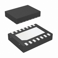
IC AMP AUDIO PWR 1.07W AB 14LLP
Manufacturer
National Semiconductor
Series
Boomer®r
Type
Class ABr
Datasheet
1.LM4992SDNOPB.pdf
(16 pages)
Specifications of LM4992SD/NOPB
Output Type
2-Channel (Stereo)
Max Output Power X Channels @ Load
1.07W x 2 @ 8 Ohm
Voltage - Supply
2.2 V ~ 5.5 V
Features
Depop, Shutdown, Thermal Protection
Mounting Type
Surface Mount
Package / Case
14-LLP
For Use With
LM4992SDBD - BOARD EVALUATION LM4992SD
Lead Free Status / RoHS Status
Lead free / RoHS Compliant
Other names
LM4992SD
LM4992SDTR
LM4992SDTR
Available stocks
Company
Part Number
Manufacturer
Quantity
Price
Company:

Part Number:
LM4992SD/NOPB
Manufacturer:
National Semiconductor
Quantity:
1 892


www.national.com
Application Information
nates possible high frequency oscillations. Care should be
taken when calculating the -3dB frequency in that an incor-
rect combination of R
20kHz. A typical combination of feedback resistor and ca-
pacitor that will not produce audio band high frequency rolloff
is R
-3dB point of approximately 320 kHz.
PCB LAYOUT GUIDELINES
This section provides practical guidelines for mixed signal
PCB layout that involves various digital/analog power and
ground traces. Designers should note that these are only
"rule-of-thumb" recommendations and the actual results will
depend heavily on the final layout.
GENERAL MIXED SIGNAL LAYOUT
RECOMMENDATION
Power and Ground Circuits
For 2 layer mixed signal design, it is important to isolate the
digital power and ground trace paths from the analog power
and ground trace paths. Star trace routing techniques (bring-
ing individual traces back to a central point rather than daisy
chaining traces together in a serial manner) can have a
major impact on low level signal performance. Star trace
3
= 20kΩ and C
4
= 25pf. These components result in a
3
and C
4
will cause rolloff before
(Continued)
12
routing refers to using individual traces to feed power and
ground to each circuit or even device. This technique will
require a greater amount of design time but will not increase
the final price of the board. The only extra parts required will
be some jumpers.
Single-Point Power / Ground Connections
The analog power traces should be connected to the digital
traces through a single point (link). A "Pi-filter" can be helpful
in minimizing High Frequency noise coupling between the
analog and digital sections. It is further recommended to put
digital and analog power traces over the corresponding digi-
tal and analog ground traces to minimize noise coupling.
Placement of Digital and Analog Components
All digital components and high-speed digital signal traces
should be located as far away as possible from analog
components and circuit traces.
Avoiding Typical Design / Layout Problems
Avoid ground loops or running digital and analog traces
parallel to each other (side-by-side) on the same PCB layer.
When traces must cross over each other do it at 90 degrees.
Running digital and analog traces at 90 degrees to each
other from the top to the bottom side as much as possible will
minimize capacitive noise coupling and cross talk.
Related parts for LM4992SD/NOPB
Image
Part Number
Description
Manufacturer
Datasheet
Request
R

Part Number:
Description:
IC,Audio Amplifier,DUAL,LLCC,14PIN,PLASTIC
Manufacturer:
National Semiconductor
Part Number:
Description:
National Semiconductor [8-Bit D/A Converter]
Manufacturer:
National Semiconductor
Datasheet:
Part Number:
Description:
National Semiconductor [Media Coprocessor]
Manufacturer:
National Semiconductor
Datasheet:
Part Number:
Description:
Digitally Controlled Tone and Volume Circuit with Stereo Audio Power Amplifier, Microphone Preamp Stage and National 3D Sound
Manufacturer:
National Semiconductor
Datasheet:
Part Number:
Description:
Digitally Controlled Tone and Volume Circuit with Stereo Audio Power Amplifier, Microphone Preamp Stage and National 3D Sound
Manufacturer:
National Semiconductor
Datasheet:
Part Number:
Description:
AC97 Rev 2 Codec with Sample Rate Conversion and National 3D Sound
Manufacturer:
National Semiconductor
Part Number:
Description:
Manufacturer:
National Semiconductor
Datasheet:
Part Number:
Description:
Manufacturer:
National Semiconductor
Datasheet:
Part Number:
Description:
General Purpose, Low Voltage, Low Power, Rail-to-Rail Output Operational Amplifiers
Manufacturer:
National Semiconductor
Datasheet:
Part Number:
Description:
8-bit 20 MSPS flash A/D converter.
Manufacturer:
National Semiconductor
Datasheet:
Part Number:
Description:
Low Noise Quad Operational Amplifier
Manufacturer:
National Semiconductor
Datasheet:
Part Number:
Description:
Quad Differential Line Receivers
Manufacturer:
National Semiconductor
Datasheet:
Part Number:
Description:
Quad High Speed Trapezoidal? Bus Transceiver
Manufacturer:
National Semiconductor
Datasheet:
Part Number:
Description:
Dual Line Receiver
Manufacturer:
National Semiconductor
Datasheet: