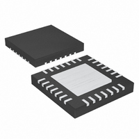
MAX9788ETI+ Maxim Integrated Products, MAX9788ETI+ Datasheet - Page 2

MAX9788ETI+
Manufacturer Part Number
MAX9788ETI+
Description
IC AMP AUDIO PWR 2.4W G 28TQFN
Manufacturer
Maxim Integrated Products
Type
Class Gr
Datasheet
1.MAX9788ETI.pdf
(13 pages)
Specifications of MAX9788ETI+
Output Type
1-Channel (Mono)
Max Output Power X Channels @ Load
2.4W x 1 @ 8 Ohm
Voltage - Supply
2.7 V ~ 5.5 V
Features
Depop, Differential Inputs, Shutdown
Mounting Type
Surface Mount
Package / Case
28-TQFN Exposed Pad
Product
Class-G
Output Power
2.4 W
Common Mode Rejection Ratio (min)
68 dB
Thd Plus Noise
0.002 %
Operating Supply Voltage
2.7 V to 5.5 V
Supply Current
8 mA
Maximum Power Dissipation
1667 mW
Maximum Operating Temperature
+ 85 C
Mounting Style
SMD/SMT
Minimum Operating Temperature
- 40 C
Supply Voltage (max)
5.5 V
Supply Voltage (min)
2.7 V
Amplifier Class
G
No. Of Channels
1
Supply Voltage Range
2.7V To 5.5V
Load Impedance
8ohm
Operating Temperature Range
-40°C To +85°C
Amplifier Case Style
TQFN
Rohs Compliant
Yes
Lead Free Status / RoHS Status
Lead free / RoHS Compliant
ABSOLUTE MAXIMUM RATINGS
(Voltages with respect to GND.)
V
PV
CPGND..................................................................-0.3V to +0.3V
OUT+, OUT-...................................(SV
IN+, IN-, FB+, FB- ......................................-0.3V to (V
C1N .........................................(PV
C1P ......................................(CPGND - 0.3V) to (CPV
FS, SHDN ...................................................-0.3V to (V
Continuous Current Into/Out of
14V
ELECTRICAL CHARACTERISTICS
(V
10µF; load connected between OUT+ and OUT-, Z
noted. Typical values are at T
Note 1: Package thermal resistances were obtained using the method described in JEDEC specification JESD51-7, using a four-
Stresses beyond those listed under “Absolute Maximum Ratings” may cause permanent damage to the device. These are stress ratings only, and functional
operation of the device at these or any other conditions beyond those indicated in the operational sections of the specifications is not implied. Exposure to
absolute maximum rating conditions for extended periods may affect device reliability.
2
GENERAL
Supply Voltage Range
Quiescent Current
Shutdown Current
Turn-On Time
Input DC Bias Voltage
Charge-Pump Oscillator
Frequency
SHDN Input Threshold
(Note 5)
SHDN Input Leakage Current
SPEAKER AMPLIFIER
Output Offset Voltage
Click-and-Pop Level
Voltage Gain
Output Voltage
CC
OUT+, OUT-, V
CC
SS
, CPV
_______________________________________________________________________________________
, SV
= V
SS
CPVDD
layer board. For detailed information on package thermal considerations, see www.maxim-ic.com/thermal-tutorial.
DD
P-P
PARAMETER
...............................................................-6V to +0.3V
.............................................................-0.3V to +6V
= V
CC
, Class G Ceramic Speaker Driver
, GND, SV
SHDN
= 3.6V, V
A
SS
= +25°C.) (Notes 2, 3)
.....................................800mA
SS
GND
- 0.3V) to (CPGND + 0.3V)
SS
SYMBOL
I
V
V
SHDN
f
= V
V
V
V
- 0.3V) to (V
I
t
OSC
BIAS
A
OUT
CC
ON
CC
OS
CP
V
CPGND
Inferred from PSRR test
SHDN = GND
Time from shutdown or power-on to full
operation
IN_ inputs (Note 4)
I
I
V
V
T
T
Peak voltage into/out of shutdown
A-weighted, 32 samples per second
(Notes 6, 7)
(Notes 4, 8)
f = 1kHz, 1% THD+N
LOAD
LOAD
A
MIN
LOAD
IH
IL
= 0V, R
CC
CC
DD
CC
= +25°C
≤ T
+ 0.3V)
+ 0.3V)
+ 0.3V)
+ 0.3V)
= 0mA (slow mode)
> 100mA (normal mode)
= 10Ω + 1µF, unless otherwise stated; T
A
IN+
≤ T
= R
MAX
CONDITIONS
IN-
Continuous Power Dissipation (T
Operating Temperature Range ...........................-40°C to +85°C
Storage Temperature Range .............................-65°C to +150°C
Lead Temperature (soldering, 10s) ................................+300°C
Bump Temperature (soldering) Reflow............................+235°C
= 10kΩ, R
CPV
Any Other Pin ..................................................................20mA
20-Bump WLP (derate 10.3mW/°C
above +70°C) (Note 1)..................................................827mW
28-Pin TQFN (derate 20.8mW/°C above +70°C) ........1667mW
DD
V
V
V
V
, CPGND, C1P, C1N, PV
CC
CC
CC
CC
FB+
= 5V
= 4.2V
= 3.6V
= 3.0V
= R
FB-
= 10kΩ, R
11.5
A
MIN
230
2.7
1.1
1.4
55
= T
A
FS
SS
MIN
= +70°C)
.................................800mA
= 100kΩ, C1 = 4.7µF, C2 =
TYP
1.24
330
to T
-67
0.3
7.1
5.9
5.1
4.2
±3
50
83
12
8
MAX
, unless otherwise
MAX
12.5
±15
±20
110
470
5.5
1.4
0.4
±1
12
5
UNITS
V
dBV
kHz
mA
mV
ms
µA
µA
dB
RMS
V
V
V


