LM4666SD National Semiconductor, LM4666SD Datasheet - Page 10
LM4666SD
Manufacturer Part Number
LM4666SD
Description
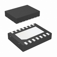
IC AMP AUDIO 1.2W STER D 14LLP
Manufacturer
National Semiconductor
Series
Boomer®r
Type
Class Dr
Datasheet
1.LM4666SD.pdf
(15 pages)
Specifications of LM4666SD
Output Type
2-Channel (Stereo)
Max Output Power X Channels @ Load
1.2W x 2 @ 8 Ohm
Voltage - Supply
2.8 V ~ 5.5 V
Features
Depop, Differential Inputs, Short-Circuit Protection, Shutdown
Mounting Type
Surface Mount
Package / Case
14-LLP
For Use With
LM4666SDBD - BOARD EVALUATION LM4666SD
Lead Free Status / RoHS Status
Lead free / RoHS Compliant
Other names
LM4666SD/NOPB
LM4666SDTR
LM4666SDTR
Available stocks
Company
Part Number
Manufacturer
Quantity
Price

Part Number:
LM4666SD
Manufacturer:
NS/国半
Quantity:
20 000
Company:
Part Number:
LM4666SD/NOPB
Manufacturer:
NS
Quantity:
525
Part Number:
LM4666SDX
Manufacturer:
NS/国半
Quantity:
20 000
Company:
Part Number:
LM4666SDX/NOPB
Manufacturer:
W
Quantity:
6 219


www.national.com
Application Information
GENERAL AMPLIFIER FUNCTION
The output signals generated by the LM4666 consist of two,
BTL connected, output signals that pulse momentarily from
near ground potential to V
outputs on a given channel can pulse independently with the
exception that they both may never pulse simultaneously as
this would result in zero volts across the BTL connected
load. The minimum width of each pulse is approximately
160ns. However, pulses on the same output can occur se-
quentially, in which case they are concatenated and appear
as a single wider pulse to achieve an effective 100% duty
cycle. This results in maximum audio output power for a
given supply voltage and load impedance. The LM4666 can
achieve much higher efficiencies than class AB amplifiers
while maintaining acceptable THD performance.
The short (160ns) drive pulses emitted at the LM4666 out-
puts means that good efficiency can be obtained with mini-
mal load inductance. The typical transducer load on an audio
amplifier is quite reactive (inductive). For this reason, the
load can act as it’s own filter, so to speak. This "filter-less"
switching amplifier/transducer load combination is much
more attractive economically due to savings in board space
and external component cost by eliminating the need for a
filter.
POWER DISSIPATION AND EFFICIENCY
In general terms, efficiency is considered to be the ratio of
useful work output divided by the total energy required to
produce it with the difference being the power dissipated,
typically, in the IC. The key here is “useful” work. For audio
systems, the energy delivered in the audible bands is con-
sidered useful including the distortion products of the input
signal. Sub-sonic (DC) and super-sonic components
(
flowing from the power supply and the audio band power
being transduced is dissipated in the LM4666 and in the
transducer load. The amount of power dissipation in the
LM4666 is very low. This is because the ON resistance of the
switches used to form the output waveforms is typically less
than 0.25Ω. This leaves only the transducer load as a po-
tential "sink" for the small excess of input power over audio
band output power. The LM4666 dissipates only a fraction of
the excess power requiring no additional PCB area or cop-
per plane to act as a heat sink.
DIFFERENTIAL AMPLIFIER EXPLANATION
As logic supply voltages continue to shrink, designers are
increasingly turning to differential analog signal handling to
preserve signal to noise ratios with restricted voltage swing.
The LM4666 is a fully differential amplifier that features
differential input and output stages. A differential amplifier
amplifies the difference between the two input signals. Tra-
ditional audio power amplifiers have typically offered only
single-ended inputs resulting in a 6dB reduction in signal to
noise ratio relative to differential inputs. The LM4666 also
offers the possibility of DC input coupling which eliminates
the two external AC coupling, DC blocking capacitors. The
LM4666 can be used, however, as a single ended input
amplifier while still retaining it’s fully differential benefits. In
fact, completely unrelated signals may be placed on the
input pins. The LM4666 simply amplifies the difference be-
tween the signals. A major benefit of a differential amplifier is
>
22kHz) are not useful. The difference between the power
DD
on each channel. The two
10
the improved common mode rejection ratio (CMRR) over
single input amplifiers. The common-mode rejection charac-
teristic of the differential amplifier reduces sensitivity to
ground offset related noise injection, especially important in
high noise applications.
PCB LAYOUT CONSIDERATIONS
As output power increases, interconnect resistance (PCB
traces and wires) between the amplifier, load and power
supply create a voltage drop. The voltage loss on the traces
between the LM4666 and the load results is lower output
power and decreased efficiency. Higher trace resistance
between the supply and the LM4666 has the same effect as
a poorly regulated supply, increase ripple on the supply line
also reducing the peak output power. The effects of residual
trace resistance increases as output current increases due
to higher output power, decreased load impedance or both.
To maintain the highest output voltage swing and corre-
sponding peak output power, the PCB traces that connect
the output pins to the load and the supply pins to the power
supply should be as wide as possible to minimize trace
resistance.
The rising and falling edges are necessarily short in relation
to the minimum pulse width (160ns), having approximately
2ns rise and fall times, typical, depending on parasitic output
capacitance. The inductive nature of the transducer load can
also result in overshoot on one or both edges, clamped by
the parasitic diodes to GND and V
EMI standpoint, this is an aggressive waveform that can
radiate or conduct to other components in the system and
cause interference. It is essential to keep the power and
output traces short and well shielded if possible. Use of
ground planes, beads, and micro-strip layout techniques are
all useful in preventing unwanted interference.
As the distance from the LM4666 and the speakers increase
the amount of EMI radiation will increase since the output
wires or traces acting as antenna become more efficient with
length. What is acceptable EMI is highly application specific.
Ferrite chip inductors placed close to the LM4666 may be
needed to reduce EMI radiation. The value of the ferrite chip
is very application specific.
POWER SUPPLY BYPASSING
As with any power amplifier, proper supply bypassing is
critical for low noise performance and high power supply
rejection ratio (PSRR). The capacitor (C
as close as possible to the LM4666. Typical applications
employ a voltage regulator with a 10µF and a 0.1µF bypass
capacitors that increase supply stability. These capacitors do
not eliminate the need for bypassing on the supply pin of the
LM4666. A 1µF tantalum capacitor is recommended.
SHUTDOWN FUNCTION
In order to reduce power consumption while not in use, the
LM4666 contains shutdown circuitry that reduces current
draw to less than 0.01µA. The trigger point for shutdown is
shown as a typical value in the Electrical Characteristics
Tables and in the Shutdown Hysteresis Voltage graphs
found in the Typical Performance Characteristics section.
It is best to switch between ground and supply for minimum
current usage while in the shutdown state. While the
LM4666 may be disabled with shutdown voltages in between
ground and supply, the idle current will be greater than the
DD
in each case. From an
S
) location should be
Related parts for LM4666SD
Image
Part Number
Description
Manufacturer
Datasheet
Request
R

Part Number:
Description:
National Semiconductor [8-Bit D/A Converter]
Manufacturer:
National Semiconductor
Datasheet:
Part Number:
Description:
National Semiconductor [Media Coprocessor]
Manufacturer:
National Semiconductor
Datasheet:
Part Number:
Description:
Digitally Controlled Tone and Volume Circuit with Stereo Audio Power Amplifier, Microphone Preamp Stage and National 3D Sound
Manufacturer:
National Semiconductor
Datasheet:
Part Number:
Description:
Digitally Controlled Tone and Volume Circuit with Stereo Audio Power Amplifier, Microphone Preamp Stage and National 3D Sound
Manufacturer:
National Semiconductor
Datasheet:
Part Number:
Description:
AC97 Rev 2 Codec with Sample Rate Conversion and National 3D Sound
Manufacturer:
National Semiconductor
Part Number:
Description:
Manufacturer:
National Semiconductor
Datasheet:
Part Number:
Description:
Manufacturer:
National Semiconductor
Datasheet:
Part Number:
Description:
General Purpose, Low Voltage, Low Power, Rail-to-Rail Output Operational Amplifiers
Manufacturer:
National Semiconductor
Datasheet:
Part Number:
Description:
8-bit 20 MSPS flash A/D converter.
Manufacturer:
National Semiconductor
Datasheet:
Part Number:
Description:
Low Noise Quad Operational Amplifier
Manufacturer:
National Semiconductor
Datasheet:
Part Number:
Description:
Quad Differential Line Receivers
Manufacturer:
National Semiconductor
Datasheet:
Part Number:
Description:
Quad High Speed Trapezoidal? Bus Transceiver
Manufacturer:
National Semiconductor
Datasheet:
Part Number:
Description:
Dual Line Receiver
Manufacturer:
National Semiconductor
Datasheet:
Part Number:
Description:
TTL to 10k ECL Level Translator with Latch
Manufacturer:
National Semiconductor
Datasheet: