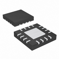
MAX9715ETE+ Maxim Integrated Products, MAX9715ETE+ Datasheet - Page 2

MAX9715ETE+
Manufacturer Part Number
MAX9715ETE+
Description
IC AMP AUDIO PWR 2.8W D 16TQFN
Manufacturer
Maxim Integrated Products
Type
Class Dr
Datasheet
1.MAX9715ETE.pdf
(13 pages)
Specifications of MAX9715ETE+
Output Type
2-Channel (Stereo)
Max Output Power X Channels @ Load
2.8W x 2 @ 4 Ohm
Voltage - Supply
4.5 V ~ 5.5 V
Features
Depop, Short-Circuit and Thermal Protection, Shutdown
Mounting Type
Surface Mount
Package / Case
16-TQFN Exposed Pad
Product
Class-D
Output Power
2.8 W
Thd Plus Noise
0.06 %
Operating Supply Voltage
5 V
Supply Current
12.8 mA
Maximum Power Dissipation
1666 mW
Maximum Operating Temperature
+ 85 C
Mounting Style
SMD/SMT
Minimum Operating Temperature
- 40 C
Supply Voltage (max)
5.5 V
Supply Voltage (min)
4.5 V
Amplifier Class
D
No. Of Channels
2
Supply Voltage Range
4.5V To 5.5V
Load Impedance
4ohm
Operating Temperature Range
-40°C To +85°C
Amplifier Case Style
TQFN
Rohs Compliant
Yes
Lead Free Status / RoHS Status
Lead free / RoHS Compliant
ABSOLUTE MAXIMUM RATINGS
V
GND to PGND .......................................................-0.3V to +0.3V
Any Other Pin to PGND ............................. -0.3V to (V
Duration of OUT__ Short Circuit to PGND or PV
Duration of OUT_+ Short Circuit between OUT_- ......Continuous
Continuous Current Into/Out of (PV
Continuous Input Current (All Other Pins) ....................... ±20mA
2.8W, Low-EMI, Stereo, Filterless Class D
Audio Amplifier
Stresses beyond those listed under “Absolute Maximum Ratings” may cause permanent damage to the device. These are stress ratings only, and functional
operation of the device at these or any other conditions beyond those indicated in the operational sections of the specifications is not implied. Exposure to
absolute maximum rating conditions for extended periods may affect device reliability.
ELECTRICAL CHARACTERISTICS
(V
OUT_+ and OUT_-, GAIN = +10.5dB, T
2
GENERAL
Supply Voltage Range
Quiescent Current
Shutdown Supply Current
Input Resistance
Turn-On Time
BIAS Voltage
CLASS D SPEAKER AMPLIFIERS
Output Offset Voltage
Maximum Speaker Amplifier Gain
(Note 3)
Power-Supply Rejection Ratio
Output Power
Total Harmonic Distortion Plus
Noise
Signal-to-Noise Ratio
Maximum Capacitive Load
Switching Frequency
DD
DD
, PV
_______________________________________________________________________________________
= PV
DD
DD
, to GND ...............................................................+6V
PARAMETER
= 5.0V, GND = PGND = 0V, V
DD
, OUT__, PGND)........1.7A
SYMBOL
A
THD+N
C
I
V
PSRR
P
SHDN
= T
SNR
L_MAX
V
V
t
f
I
R
BIAS
A
OUT
DD
ON
SW
DD
OS
IN
V
SHDN
MIN
DD
to T
= V
....Continuous
Inferred from PSRR test
No load
V
T
T
GAIN = 0
GAIN = 1
V
THD+N = 1%
THD+N = 10%
f = 1kHz
P
P
Average frequency in spread-spectrum
operation
MAX
A
A
SHDN
IN_
OUT
OUT
DD
DD
= +25°C
= T
, C
, unless otherwise noted. Typical values are at T
= 0V
= 1W, BW = 22Hz to 22kHz
= 1W, A-weighted
+ 0.3V)
MIN
= 0V
BIAS
to T
= 1μF, speaker impedance = 8Ω in series with 68μH connected between
MAX
CONDITIONS
Continuous Power Dissipation (T
Operating Temperature Range ...........................-40°C to +85°C
Storage Temperature Range .............................-65°C to +150°C
Junction Temperature ......................................................+150°C
Lead Temperature (soldering, 10s) .................................+300°C
PV
5.5V
f = 1kHz, 100mV
f = 20kHz, 100mV
R
R
R
R
R
R
16-Pin TQFN-EP (derate 20.8mW/°C above +70°C)..1666mW
L
L
L
L
L
L
DD
= 8Ω
= 4Ω
= 8Ω
= 4Ω
= 8Ω, P
= 4Ω, P
or V
DD
OUT
OUT
= 4.5V to
= 1.2W
= 2W
P-P
P-P
MIN
52.4
1.00
4.5
6.5
A
A
= +25°C.) (Notes 1, 2)
= +70°C)
TYP
12.8
12.6
10.5
0.06
0.07
1.22
200
0.1
1.8
9.0
1.4
2.3
1.7
2.8
10
25
75
71
60
89
93
MAX
13.5
1.40
5.5
16
45
70
2
UNITS
MHz
mA
mV
ms
μA
kΩ
dB
dB
dB
pF
W
%
V
V


