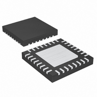
MAX9703ETJ+ Maxim Integrated Products, MAX9703ETJ+ Datasheet - Page 11

MAX9703ETJ+
Manufacturer Part Number
MAX9703ETJ+
Description
IC AMP AUDIO PWR 18W MONO 32TQFN
Manufacturer
Maxim Integrated Products
Type
Class Dr
Datasheet
1.MAX9703ETJ.pdf
(20 pages)
Specifications of MAX9703ETJ+
Output Type
1-Channel (Mono)
Max Output Power X Channels @ Load
18W x 1 @ 16 Ohm
Voltage - Supply
10 V ~ 25 V
Features
Depop, Differential Inputs, Mute, Short-Circuit and Thermal Protection, Shutdown
Mounting Type
Surface Mount
Package / Case
32-TQFN Exposed Pad
Product
Class-D
Output Power
15 mW
Common Mode Rejection Ratio (min)
60 dB
Thd Plus Noise
0.07 %
Operating Supply Voltage
10 V to 25 V
Supply Current
14 mA
Maximum Power Dissipation
1702 mW
Maximum Operating Temperature
+ 85 C
Mounting Style
SMD/SMT
Input Signal Type
Differential
Minimum Operating Temperature
- 40 C
Supply Voltage (max)
25 V
Supply Voltage (min)
10 V
Amplifier Class
D
No. Of Channels
1
Supply Voltage Range
10V To 25V
Load Impedance
4ohm
Operating Temperature Range
-40°C To +85°C
Amplifier Case Style
TQFN
Rohs Compliant
Yes
Lead Free Status / RoHS Status
Lead free / RoHS Compliant
The MAX9703/MAX9704 feature an internally set, logic-
selectable gain. The G1 and G2 logic inputs set the
gain of the MAX9703/MAX9704 speaker amplifier
(Table 2).
Unlike a Class AB amplifier, the output offset voltage of
Class D amplifiers does not noticeably increase quies-
cent current draw when a load is applied. This is due to
the power conversion of the Class D amplifier. For
example, an 8mV DC offset across an 8Ω load results
in 1mA extra current consumption in a class AB device.
In the Class D case, an 8mV offset into 8Ω equates
to an additional power drain of 8µW. Due to the high
efficiency of the Class D amplifier, this represents an
additional quiescent current draw of: 8µW/(V
which is in the order of a few microamps.
The MAX9703/MAX9704 feature a differential input struc-
ture, making them compatible with many CODECs, and
offering improved noise immunity over a single-ended
input amplifier. In devices such as PCs, noisy digital sig-
nals can be picked up by the amplifier’s input traces.
The signals appear at the amplifiers’ inputs as common-
mode noise. A differential input amplifier amplifies the
difference of the two inputs, any signal common to both
inputs is canceled.
The MAX9703/MAX9704 can be configured as single-
ended input amplifiers by capacitively coupling either
input to AGND and driving the other input (Figure 4).
An input capacitor, C
impedance of the MAX9703/MAX9704, forms a high-
pass filter that removes the DC bias from an incoming
signal. The AC-coupling capacitor allows the amplifier
to bias the signal to an optimum DC level. Assuming
Table 2. Gain Selection
G1
0
0
1
1
______________________________________________________________________________________
IN
, in conjunction with the input
G2
Spread-Spectrum, Class D Amplifiers
0
1
0
1
Component Selection
10W Stereo/15W Mono, Filterless,
Single-Ended Input
Input Amplifier
Gain Selection
Differential Input
Output Offset
GAIN (dB)
DD
Input Filter
29.6
19.1
13
16
/100
✕
η),
zero-source impedance, the -3dB point of the highpass
filter is given by:
Choose C
of interest. Setting f
quency response of the amplifier. Use capacitors with
dielectrics that have low-voltage coefficients, such as
tantalum or aluminum electrolytic. Capacitors with high-
voltage coefficients, such as ceramics, may result in
increased distortion at low frequencies.
Use capacitors with an ESR less than 100mΩ for opti-
mum performance. Low-ESR ceramic capacitors mini-
mize the output resistance of the charge pump. For
best performance over the extended temperature
range, select capacitors with an X7R dielectric.
The value of the flying capacitor (C1) affects the load
regulation and output resistance of the charge pump. A
C1 value that is too small degrades the device’s ability to
provide sufficient current drive. Increasing the value of
C1 improves load regulation and reduces the charge-
pump output resistance to an extent. Above 1µF, the on-
resistance of the switches and the ESR of C1 and C2
dominate.
The output capacitor value and ESR directly affect the rip-
ple at CHOLD. Increasing C2 reduces output ripple.
Likewise, decreasing the ESR of C2 reduces both ripple
and output resistance. Lower capacitance values can be
used in systems with low maximum output power levels.
The MAX9703/MAX9704 do not require an output filter
and can pass FCC emissions standards with unshield-
ed speaker cables. However, output filtering can be
Figure 4. Single-Ended Input
IN
SINGLE-ENDED
Charge-Pump Capacitor Selection
so f
AUDIO INPUT
-3dB
0.47μF
f
- 3dB
-3dB
is well below the lowest frequency
0.47μF
=
too high affects the low-fre-
2
π
R C
IN+
IN-
IN IN
1
Flying Capacitor (C1)
MAX9703/
MAX9704
Hold Capacitor (C2)
Output Filter
11


