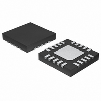
MAX4409ETP+ Maxim Integrated Products, MAX4409ETP+ Datasheet - Page 2

MAX4409ETP+
Manufacturer Part Number
MAX4409ETP+
Description
IC AMP AUDIO .08W STER AB 20TQFN
Manufacturer
Maxim Integrated Products
Series
DirectDrive™r
Type
Class ABr
Datasheet
1.MAX4409ETP.pdf
(20 pages)
Specifications of MAX4409ETP+
Output Type
Headphones, 2-Channel (Stereo)
Max Output Power X Channels @ Load
80mW x 2 @ 16 Ohm
Voltage - Supply
1.8 V ~ 3.6 V
Features
Depop, Short-Circuit and Thermal Protection, Shutdown
Mounting Type
Surface Mount
Package / Case
20-TQFN Exposed Pad
Product
General Purpose Audio Amplifiers
Output Power
80 mW
Common Mode Rejection Ratio (min)
96 dB
Thd Plus Noise
0.002 %
Operating Supply Voltage
1.8 V to 3.6 V
Supply Current
5 mA
Maximum Power Dissipation
2051 mW
Maximum Operating Temperature
+ 85 C
Mounting Style
SMD/SMT
Input Bias Current (max)
0 nA
Input Offset Voltage
0.5 mV
Input Signal Type
Differential
Minimum Operating Temperature
- 40 C
Supply Voltage (max)
3.6 V
Supply Voltage (min)
1.8 V
Amplifier Class
AB
No. Of Channels
2
Supply Voltage Range
1.8V To 3.6V
Load Impedance
16ohm
Operating Temperature Range
-40°C To +85°C
Amplifier Case Style
TQFN
Rohs Compliant
Yes
Lead Free Status / RoHS Status
Lead free / RoHS Compliant
ABSOLUTE MAXIMUM RATINGS
PGND to SGND .....................................................-0.3V to +0.3V
PV
PV
PV
PV
IN_ and COM to SGND.................................SV
IN_ to COM .....................................(COM + 2V) to (COM - 0.3V)
SHDN_ to SGND........................(SGND - 0.3V) to (SV
OUT_ to SGND ............................(SV
C1P to PGND.............................(PGND - 0.3V) to (PV
C1N to PGND .............................(PV
80mW, DirectDrive, Stereo Headphone
Amplifier with Common-Mode Sense
Stresses beyond those listed under “Absolute Maximum Ratings” may cause permanent damage to the device. These are stress ratings only, and functional
operation of the device at these or any other conditions beyond those indicated in the operational sections of the specifications is not implied. Exposure to
absolute maximum rating conditions for extended periods may affect device reliability.
ELECTRICAL CHARACTERISTICS
(V
T
2
Note 1: Package thermal resistances were obtained using the method described in JEDEC specification JESD51-7, using a 4-layer
Supply Voltage Range
Quiescent Supply Current
Shutdown Supply Current
SHDN Thresholds
SHDN Input Leakage Current
SHDN to Full Operation
CHARGE PUMP
Oscillator Frequency
AMPLIFIERS
Input Offset Voltage
Input Bias Current
COM Bias Current
Equivalent Input Offset Current
COM Input Range
Common-Mode Rejection Ratio
Power-Supply Rejection Ratio
Output Power
MAX
PVDD
DD
SS
DD
SS
_______________________________________________________________________________________
, unless otherwise noted. Typical values are at T
to SV
and SV
to SV
and SV
= V
board. For detailed information on package thermal considerations see www.maxim-ic.com/thermal-tutorial.
SS
PARAMETER
DD .................................................................
SVDD
SS
DD
.........................................................-0.3V to +0.3V
to PGND or SGND ..........................-4V to +0.3V
to PGND or SGND .........................-0.3V to +4V
= 3V, V
PGND
= V
SGND
SS
SS
SYMBOL
- 0.3V) to (PGND + 0.3V)
CMRR
I
- 0.3V) to (SV
V
PSRR
I
P
I
SHDN
t
f
V
V
COM
BIAS
I
SON
OSC
I
COM
OUT
DD
= 0, SHDN = SV
OS
DD
OS
SS
-0.3V to +0.3V
to (SV
Guaranteed by PSRR test
SHDN = GND
V
V
R
I
Inferred from CMRR test
-500mV ≤ V
1.8V ≤ V
V
200mV
THD+N = 1%, T
OS
IH
IL
DD
L
DD
DD
DD
= 32Ω
A
= (I
= 3.0V,
DD
= +25°C.) (Note 2)
+ 0.3V)
+ 0.3V)
+ 0.3V)
P-P
BIAS(INR)
DD
DD
- 1V)
ripple (Note 4)
, C1 = C2 = 2.2µF, R
COM
≤ 3.6V
A
CONDITIONS
≤ +500mV, R
+ I
= +25°C
BIAS(INL)
Output Short Circuit to GND or V
Thermal Limits (Note 1)
Continuous Power Dissipation (T
Junction Temperature ......................................................+150°C
Operating Temperature Range ...........................-40°C to +85°C
Storage Temperature Range .............................-65°C to +150°C
Lead Temperature (soldering, 10s) .................................+300°C
20-Pin Thin QFN Multilayer (derate 25.6mW/°C
θ
θ
JA
JC
above +70°C)..........................................................2051mW
................................................................................39°C/W
...............................................................................5.7°C/W
- I
SOURCE
DC (Note 3)
f
f
R
R
COM
RIPPLE
RIPPLE
L
L
IN
= 32Ω
= 16Ω
) / 2
= R
= 1kHz
= 20kHz
≤ 10Ω
F
= R1 = R2 = 10kΩ, R
-1400
SV
0.7 x
-700
-500
MIN
272
1.8
75
75
55
-1
DD
DD
A
= +70°C)
...........................Continuous
-100
-200
TYP
175
320
0.5
±2
96
86
76
48
65
80
5
6
L
= ∞, T
SV
MAX
+500
0.3 x
368
3.6
8.4
2.4
+1
10
0
0
DD
A
= T
UNITS
kHz
mW
mA
mV
mV
dB
dB
MIN
µA
µA
nA
nA
nA
µs
V
V
to


