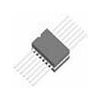
LM124AWG/883 National Semiconductor, LM124AWG/883 Datasheet - Page 12

LM124AWG/883
Manufacturer Part Number
LM124AWG/883
Description
Manufacturer
National Semiconductor
Type
General Purpose Amplifierr
Datasheet
1.LM124AWG883.pdf
(28 pages)
Specifications of LM124AWG/883
Rail/rail I/o Type
No
Number Of Elements
4
Unity Gain Bandwidth Product
1MHz
Slew Rate
0.1V/us
Common Mode Rejection Ratio
70dB
Input Offset Voltage
2mV
Input Bias Current
10nA
Single Supply Voltage (typ)
5/9/12/15/18/24/28V
Dual Supply Voltage (typ)
±3/±5/±9/±12/±15V
Power Dissipation
700mW
Voltage Gain In Db
93.98dB
Power Supply Rejection Ratio
65dB
Power Supply Requirement
Single/Dual
Shut Down Feature
No
Single Supply Voltage (min)
3V
Single Supply Voltage (max)
32V
Dual Supply Voltage (min)
±1.5V
Dual Supply Voltage (max)
±16V
Technology
Bipolar
Operating Temp Range
-55C to 125C
Operating Temperature Classification
Military
Mounting
Surface Mount
Pin Count
14
Package Type
CPAK
Dc
11+
Lead Free Status / Rohs Status
Not Compliant
Available stocks
Company
Part Number
Manufacturer
Quantity
Price
Company:
Part Number:
LM124AWG/883
Manufacturer:
NSC
Quantity:
1 400
Note 2: Absolute Maximum Ratings indicate limits beyond which damage to the device may occur. Operating Ratings indicate conditions for which the device is
functional, but do not guarantee specific performance limits. For guaranteed specifications and test conditions, see the Electrical Characteristics. The guaranteed
specifications apply only for the test conditions listed. Some performance characteristics may degrade when the device is not operated under the listed test
conditions.
Note 3: The maximum power dissipation must be derated at elevated temperatures and is dictated by T
(maximum junction temperature), ThetaJ
(package
Jmax
A
junction to ambient thermal resistance), and T
(ambient temperature). The maximum allowable power dissipation at any temperature is P
= (T
- T
)/
A
Dmax
Jmax
A
ThetaJ
or the number given in the Absolute Maximum Ratings, whichever is lower.
A
Note 4: Short circuits from the output to V+ can cause excessive heating and eventual destruction. When considering short circuits to ground, the maximum
output current is approximately 40mA independent of the magnitude of V+. At values of supply voltage in excess of +15V
, continuous short-circuits can exceed
DC
the power dissipation ratings and cause eventual destruction. Destructive dissipation can result from simultaneous shorts on all amplifiers.
Note 5: This input current will only exist when the voltage at any of the input leads is driven negative. It is due to the collector-base junction of the input PNP
transistors becoming forward biased and thereby acting as input diode clamps. In addition to this diode action, there is also lateral NPN parasitic transistor action
on the IC chip. This transistor action can cause the output voltages of the op amps to go to the V+ voltage level (or to ground for a large overdrive) for the time
duration that an input is driven negative. This is not destructive and normal output states will re-establish when the input voltage, which was negative, again
returns to a value greater than -0.3V
(at 25°C).
DC
Note 6: Human body model, 1.5 kΩ in series with 100 pF.
Note 7: Guaranteed by V
tests.
IO
Note 8: Datalog reading in K=V/mV
Note 9: Guaranteed, not tested
Note 10: Calculated parameters
Note 11: Pre and post irradiation limits are identical to those listed under AC and DC electrical characteristics except as listed in the Post Radiation Limits Table.
These parts may be dose rate sensitive in a space environment and demonstrate enhanced low dose rate effect. Radiation end point limits for the noted parameters
are guaranteed only for the conditions as specified in MIL-STD-883, Method 1019
Note 12: Low dose rate testing has been performed on a wafer-by-wafer basis, per test method 1019 condition D of MIL-STD-883, with no enhanced low dose
rate sensitivity (ELDRS) effect.
Note 13: The direction of the input current is out of the IC due to the PNP input stage. This current is essentially constant, independent of the state of the output
so no loading change exists on the input lines.
Note 14: The input common-mode voltage of either input signal voltage should not be allowed to go negative by more than 0.3V (at 25°C). The upper end of the
common-mode voltage range is V+ −1.5V (at 25°C), but either or both inputs can go to +32V without damage independent of the magnitude of V+.
Note 15: Due to proximity of external components, insure that coupling is not originating via stray capacitance between these external parts. This typically can
be detected as this type of capacitance increases at higher frequencies.
Typical Performance Characteristics
Input Voltage Range
Input Current
20108034
20108035
www.national.com
12


