LM4995SDX/NOPB National Semiconductor, LM4995SDX/NOPB Datasheet
LM4995SDX/NOPB
Specifications of LM4995SDX/NOPB


Related parts for LM4995SDX/NOPB


LM4995SDX/NOPB Summary of contents
Page 1
... The LM4995 is unity-gain stable and can be configured by external gain-setting resistors. Typical Application FIGURE 1. Typical Audio Amplifier Application Circuit Boomer® registered trademark of National Semiconductor Corporation. © 2009 National Semiconductor Corporation LM4995 Key Specifications ■ ...
Page 2
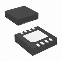
Connection Diagrams TM Package Top View Order Number LM4995TM See NS Package Number TMD09AAA SD Package Top View Order Number LM4995SD See NS Package Number SDA08A www.national.com 20159903 V - Die Traceability G - Boomer Family 20159957 Z - Assembly ...
Page 3
... Absolute Maximum Ratings If Military/Aerospace specified devices are required, please contact the National Semiconductor Sales Office/ Distributors for availability and specifications. Supply Voltage (Note 10) Storage Temperature Input Voltage Power Dissipation (Note 3, Note 11) ESD Susceptibility (Note 4) ESD Susceptibility (Note 5) Electrical Characteristics V The following specifications apply for the circuit shown in Figure 1, unless otherwise specified. Limits apply for T ...
Page 4
Electrical Characteristics V The following specifications apply for the circuit shown in Figure 1, unless otherwise specified. Limits apply for T Symbol Parameter I Quiescent Power Supply Current DD I Shutdown Current SD V Output Offset Voltage OS P Output ...
Page 5
Typical Performance Characteristics THD+N vs Output Power = 8Ω 3V THD+N vs Output Power = 8Ω 5V THD+N vs Output Power V = 3.6V 20159918 THD+N vs Frequency ...
Page 6
THD+N vs Frequency V = 3.6V 1kHz 300mW O PSRR vs Frequency www.national.com = 8Ω, L 20159941 = 8Ω 20159950 6 THD+N vs Frequency = 8Ω ...
Page 7
PSRR vs Frequency = 8Ω 5V 20159951 Power Dissipation vs Output Power = 8Ω 3.6V Power Dissipation vs Output Power Power Dissipation vs Output Power ...
Page 8
Output Level vs Frequency Response (Three different caps) Shutdown Voltage 3.6V DD www.national.com 20159906 SDIH 20159947 8 Shutdown Voltage V SDIH 20159936 Shutdown Voltage V SDIH 20159937 ...
Page 9
Shutdown Voltage V SDIL 20159939 Shutdown Voltage V SDIL 20159940 Shutdown Voltage 3.6V DD Output Power vs Supply Voltage = 8Ω SDIL 20159948 20159907 www.national.com ...
Page 10
Application Information BRIDGE CONFIGURATION EXPLANATION As shown in Figure 1, the LM4995 has two internal opera- tional amplifiers. The first amplifier's gain is externally config- urable, while the second amplifier is internally fixed in a unity- gain, inverting configuration. The ...
Page 11
Figure 1. The input coupling capacitor, C high pass filter which limits low frequency response. This val- ue should be chosen based on needed frequency response for a few ...
Page 12
FIGURE 3. DIFFERENTIAL AMPLIFIER CONFIGURATION FOR LM4995 www.national.com FIGURE 2. HIGHER GAIN AUDIO AMPLIFIER 12 201599d4 201599d5 ...
Page 13
FIGURE 4. REFERENCE DESIGN BOARD SCHEMATIC 13 201599d6 www.national.com ...
Page 14
PCB LAYOUT GUIDELINES This section provides practical guidelines for mixed signal PCB layout that involves various digital/analog power and ground traces. Designers should note that these are only "rule-of-thumb" recommendations and the actual results will depend heavily on the final ...
Page 15
Revision History Rev 1.0 1.1 1.2 1.3 1.4 Date 04/05/06 Initial WEB released of the datasheet. 05/17/06 Added the SD package. 08/07/06 08/22/06 Edited the THD+N Typical values on the 3 EC tables, then re-released the the ...
Page 16
Physical Dimensions X1 = 1.215± 0.03mm X2 = 1.215 ± 0.03mm X3 = 0.6 ± 0.075mm www.national.com inches (millimeters) unless otherwise noted TM Package Order Number LM4995TM NS Package Number TMD09AAA SDPackage Order Number LM4995SD NS Package Number SDA08A 16 ...
Page 17
Notes 17 www.national.com ...
Page 18
... For more National Semiconductor product information and proven design tools, visit the following Web sites at: Products Amplifiers www.national.com/amplifiers Audio www.national.com/audio Clock and Timing www.national.com/timing Data Converters www.national.com/adc Interface www.national.com/interface LVDS www.national.com/lvds Power Management www.national.com/power Switching Regulators www.national.com/switchers LDOs www.national.com/ldo LED Lighting www ...