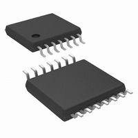
LM48100QMH/NOPB National Semiconductor, LM48100QMH/NOPB Datasheet - Page 12

LM48100QMH/NOPB
Manufacturer Part Number
LM48100QMH/NOPB
Description
IC AMP AUDIO PWR 1.6W 14ETSSOP
Manufacturer
National Semiconductor
Series
Boomer®, PowerWise®r
Type
Class ABr
Datasheet
1.LM48100QMHENOPB.pdf
(24 pages)
Specifications of LM48100QMH/NOPB
Output Type
1-Channel (Mono)
Max Output Power X Channels @ Load
1.6W x 1 @ 8 Ohm
Voltage - Supply
3 V ~ 5.5 V
Features
Depop, I²C, Input Multiplexer, Short-Circuit and Thermal Protection, Shutdown, Volume Control
Mounting Type
Surface Mount
Package / Case
14-TSSOP Exposed Pad, 14-eTSSOP 14-HTSSOP
Amplifier Class
AB
No. Of Channels
1
Output Power
1.3W
Supply Voltage Range
3V To 5.5V
Load Impedance
8ohm
Operating Temperature Range
-40°C To +105°C
Amplifier Case Style
TSSOP
Rohs Compliant
Yes
Lead Free Status / RoHS Status
Lead free / RoHS Compliant
Other names
LM48100QMH
www.national.com
Application Information
WRITE-ONLY I
The LM48100Q is controlled through an I
interface that consists of a serial data line (SDA) and a serial
clock (SCL). The clock line is uni-directional. The data line is
bi-directional (open drain). The LM48100Q and the master
can communicate at clock rates up to 400kHz. Figure 2 shows
the I
be stable during the HIGH period of SCL. The LM48100Q is
a transmit/receive slave-only device, reliant upon the master
to generate the SCL signal. Each transmission sequence is
framed by a START condition and a STOP condition (Figure
3). Each data word, device address and data, transmitted
over the bus is 8 bits long and is always followed by an ac-
knowledge pulse (Figure 4). The LM48100Q device address
is 111110X, where X is determined by ADR (Table 2). ADR =
1 sets the device address to 1111101. ADR = 0 sets the de-
vice address to 1111100.
I
The I
the transition of SDA from HIGH to LOW while SCL is HIGH,
2
C BUS FORMAT
2
2
C interface timing diagram. Data on the SDA line must
C bus format is shown in Figure 4. The START signal,
2
C COMPATIBLE INTERFACE
2
C compatible serial
FIGURE 3. Start and Stop Diagram
FIGURE 2. I
2
C Timing Diagram
12
is generated, alerting all devices on the bus that a device ad-
dress is being written to the bus.
The 7-bit device address is written to the bus, most significant
bit (MSB) first, followed by the R/W bit. R/W = 0 indicates the
master is writing to the slave device, RW = 1 indicates the
master wants to read data from the slave device. Set R/W =
0; the LM48100Q is a WRITE-ONLY device and will not re-
spond the R/W = 1. The data is latched in on the rising edge
of the clock. Each address bit must be stable while SCL is
HIGH. After the last address bit is transmitted, the master de-
vice releases SDA, during which time, an acknowledge clock
pulse is generated by the slave device. If the LM48100Q re-
ceives the correct address, the device pulls the SDA line low,
generating an acknowledge bit (ACK).
Once the master device registers the ACK bit, the 8-bit reg-
ister data word is sent. Each data bit should be stable while
SCL is HIGH. After the 8-bit register data word is sent, the
LM48100Q sends another ACK bit. Following the acknowl-
edgement of the register data word, the master issues a
STOP bit, allowing SDA to go high.
300758g8
30075867


