MAX9725AETC+T Maxim Integrated Products, MAX9725AETC+T Datasheet - Page 2
MAX9725AETC+T
Manufacturer Part Number
MAX9725AETC+T
Description
IC AMP AUDIO .025W STER 12TQFN
Manufacturer
Maxim Integrated Products
Series
DirectDrive™r
Type
Class ABr
Datasheet
1.MAX9725CETCT.pdf
(17 pages)
Specifications of MAX9725AETC+T
Output Type
Headphones, 2-Channel (Stereo)
Max Output Power X Channels @ Load
25mW x 2 @ 16 Ohm
Voltage - Supply
900 mV ~ 1.8 V
Features
Depop, Short-Circuit Protection, Shutdown
Mounting Type
Surface Mount
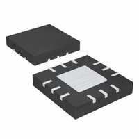
Package / Case
12-TQFN Exposed Pad
Lead Free Status / RoHS Status
Lead free / RoHS Compliant


ABSOLUTE MAXIMUM RATINGS
SGND to PGND .....................................................-0.3V to +0.3V
V
V
C1P to PGND..............................................-0.3V to (V
C1N to PGND............................................(PV
V
OUTR, OUTL, INR, INL to SGND
OUTR, OUTL to SGND
INR, INL to SGND (MAX9725E)...................................-4V to +4V
1V, Low-Power, DirectDrive, Stereo Headphone
Amplifier with Shutdown
Stresses beyond those listed under “Absolute Maximum Ratings” may cause permanent damage to the device. These are stress ratings only, and functional
operation of the device at these or any other conditions beyond those indicated in the operational sections of the specifications is not implied. Exposure to
absolute maximum rating conditions for extended periods may affect device reliability.
ELECTRICAL CHARACTERISTICS (MAX9725A–MAX9725D)
(V
wise noted. Typical values are at T
2
Supply Voltage Range
Quiescent Supply Current
Shutdown Current
Shutdown to Full Operation
SHDN Thresholds
SHDN Input Leakage Current
CHARGE PUMP
Oscillator Frequency
AMPLIFIERS
Voltage Gain
Gain Match
Total Output Offset Voltage
Input Resistance
Power-Supply Rejection Ratio
Output Power (Note 3)
DD
SS
SS
(MAX9725A–MAX9725D)..............(V
(MAX9725E) ..................................(V
DD
, PV
to PV
_______________________________________________________________________________________
to SGND or PGND ............................................-0.3V to +2V
= 1.5V, V
SS
SS
PARAMETER
to GND ....................................................+0.3V to -2V
...........................................................-0.3V to +0.3V
PGND
= V
SGND
= 0V, V
SYMBOL
A
I
= +25°C.) (See the Functional Diagrams. ) (Note 1)
PSRR
I
P
SHDN
f
V
LEAK
ΔA
V
t
I
V
OSC
R
V
A
ON
OUT
DD
SS
SS
SHDN
DD
OS
IH
IN
IL
V
V
- 0.3V) to (V
- 0.3V) to (V
= 1.5V, V
SS
Guaranteed by PSRR test
Both channels active
V
V
V
V
MAX9725A
MAX9725B
MAX9725C
MAX9725D
Input AC-coupled,
R
T
V
100mV
V
V
V
A
SHDN
DD
DD
DD
DD
DD
DD
DD
L
- 0.3V) to +0.3V
= 32Ω to GND,
= +25°C
= 0.9V to 1.8V
= 0.9V to 1.8V
= 0.9V to 1.8V (Note 2)
= 0.9V to 1.8V, T
= 1.5V
= 1.0V, R
= 0.9V, R
P-P
= 0V
DD
DD
DD
SS
ripple
+ 0.3V)
+ 0.3V)
+ 0.3V)
= V
L
L
PVSS
= 32Ω
= 32Ω
CONDITIONS
, C1 = C2 = 1µF, C
A
= +25°C
SHDN to SGND or PGND .........................................-0.3V to +4V
Output Short-Circuit Current ......................................Continuous
Continuous Power Dissipation (T
Junction Temperature ......................................................+150°C
Operating Temperature Range ...........................-40°C to +85°C
Storage Temperature Range .............................-65°C to +150°C
Bump Temperature (soldering) Reflow............................+230°C
Lead Temperature (soldering, 10s) .................................+300°C
MAX9725A/MAX9725D
MAX9725B
MAX9725C
f
f
R
R
IN
IN
12-Bump UCSP (derate 6.5mW/°C above +70°C)....518.8mW
12-Pin Thin QFN (derate 16.9mW/°C above +70°C) ..1349.1mW
L
L
T
T
= 1kHz
= 20kHz
= 32Ω
= 16Ω
A
A
= +25°C
= -40°C to +85°C
IN
= 1µF, R
L
= ∞, T
0.7 x V
-2.04
-1.53
-1.02
-4.08
MIN
493
0.9
15
60
10
A
A
= +70°C)
= T
DD
±0.45
MIN
-2.00
-1.00
-4.00
±0.5
±0.3
±0.6
TYP
-1.5
180
580
2.1
0.6
25
80
70
62
20
25
7
6
to T
0.3 x V
MAX,
±1.05
±1.58
-1.96
-1.47
-0.98
-3.92
MAX
±2.1
667
1.8
3.3
10
30
±1
35
DD
unless other-
UNITS
kHz
mW
mA
V/V
mV
µA
µA
kΩ
dB
µs
%
V
V
Related parts for MAX9725AETC+T
Image
Part Number
Description
Manufacturer
Datasheet
Request
R

Part Number:
Description:
Stereo Headphone Amplifier
Manufacturer:
Maxim Integrated Products
Datasheet:

Part Number:
Description:
Max9725 1v, Low-power, Directdrive, Stereo Headphone Amplifier With Shutdown
Manufacturer:
Maxim Integrated Products, Inc.
Datasheet:
Part Number:
Description:
MAX7528KCWPMaxim Integrated Products [CMOS Dual 8-Bit Buffered Multiplying DACs]
Manufacturer:
Maxim Integrated Products
Datasheet:
Part Number:
Description:
Single +5V, fully integrated, 1.25Gbps laser diode driver.
Manufacturer:
Maxim Integrated Products
Datasheet:
Part Number:
Description:
Single +5V, fully integrated, 155Mbps laser diode driver.
Manufacturer:
Maxim Integrated Products
Datasheet:
Part Number:
Description:
VRD11/VRD10, K8 Rev F 2/3/4-Phase PWM Controllers with Integrated Dual MOSFET Drivers
Manufacturer:
Maxim Integrated Products
Datasheet:
Part Number:
Description:
Highly Integrated Level 2 SMBus Battery Chargers
Manufacturer:
Maxim Integrated Products
Datasheet:
Part Number:
Description:
Current Monitor and Accumulator with Integrated Sense Resistor; ; Temperature Range: -40°C to +85°C
Manufacturer:
Maxim Integrated Products
Part Number:
Description:
TSSOP 14/A°/RS-485 Transceivers with Integrated 100O/120O Termination Resis
Manufacturer:
Maxim Integrated Products
Part Number:
Description:
TSSOP 14/A°/RS-485 Transceivers with Integrated 100O/120O Termination Resis
Manufacturer:
Maxim Integrated Products
Part Number:
Description:
QFN 16/A°/AC-DC and DC-DC Peak-Current-Mode Converters with Integrated Step
Manufacturer:
Maxim Integrated Products
Part Number:
Description:
TDFN/A/65V, 1A, 600KHZ, SYNCHRONOUS STEP-DOWN REGULATOR WITH INTEGRATED SWI
Manufacturer:
Maxim Integrated Products
Part Number:
Description:
Integrated Temperature Controller f
Manufacturer:
Maxim Integrated Products
Part Number:
Description:
SOT23-6/I°/45MHz to 650MHz, Integrated IF VCOs with Differential Output
Manufacturer:
Maxim Integrated Products
Part Number:
Description:
SOT23-6/I°/45MHz to 650MHz, Integrated IF VCOs with Differential Output
Manufacturer:
Maxim Integrated Products