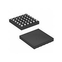
MAX97000EWA+T Maxim Integrated Products, MAX97000EWA+T Datasheet - Page 5

MAX97000EWA+T
Manufacturer Part Number
MAX97000EWA+T
Description
IC AUDIO SUBSYSTEM 25WLP
Manufacturer
Maxim Integrated Products
Series
DirectDrive™r
Type
Class Dr
Datasheet
1.MAX97000EWAT.pdf
(34 pages)
Specifications of MAX97000EWA+T
Output Type
1-Channel (Mono) with Stereo Headphones
Max Output Power X Channels @ Load
930mW x 1 @ 8 Ohm; 40mW x 2 @ 16 Ohm
Voltage - Supply
2.7 V ~ 5.5 V
Features
Depop, Differential Inputs, I²C, Mute, Shutdown, Volume Control
Mounting Type
Surface Mount
Package / Case
25-WLP
Product
Class-D
Output Power
725 mW
Available Set Gain
12 dB
Common Mode Rejection Ratio (min)
32 dB to 55 dB
Thd Plus Noise
0.05 %
Operating Supply Voltage
2.7 V to 5.5 V
Supply Current
0.4 mA to 1.45 mA
Maximum Power Dissipation
850 mW
Maximum Operating Temperature
+ 80 C
Mounting Style
SMD/SMT
Audio Load Resistance
41.2 KOhms
Input Signal Type
Differential
Minimum Operating Temperature
- 40 C
Output Signal Type
Differential
Supply Voltage (max)
5.5 V
Supply Voltage (min)
2.7 V
Lead Free Status / RoHS Status
Lead free / RoHS Compliant
Other names
MAX97000EWA+T
(Voltages with respect to GND.)
VDD, HPVDD ........................................................-0.3V to +2.2V
PVDD, LDOIN .......................................................-0.3V to +6.0V
PGND ...................................................................-0.1V to +0.1V
HPVSS .................................................................-2.2V to + 0.3V
C1N ..................................... (HPVSS - 0.3V) to (HPVDD + 0.3V)
C1P ..........................................................- 0.3V to (VDD + 0.3V)
HPL, HPR ............................. (HPVSS - 0.3V) to (HPVDD +0.3V)
INA1, INA2, INB1, INB2, BIAS .............................-0.3V to +6.0V
SDA, SCL, SHDN .................................................-0.3V to +6.0V
COM1, COM2, NC1, NC2,
Continuous Current In/Out of PVDD, PGND, OUT_ ...... Q800mA
Continuous Current In/Out of HPR, HPL,
ELECTRICAL_CHARACTERISTICS
(V
HPLVOL = HPRVOL = SPKVOL = 0dB, speaker loads (Z
nected from HPL or HPR to GND. SDA and SCL pullup voltage = 1.8V. Z
= 1FF. T
ABSOLUTE_MAXIMUM_RATINGS
Stresses beyond those listed under “Absolute Maximum Ratings” may cause permanent damage to the device. These are stress ratings only, and functional
operation of the device at these or any other conditions beyond those indicated in the operational sections of the specifications is not implied. Exposure to absolute
maximum rating conditions for extended periods may affect device reliability.
Speaker Amplifier Supply-
Voltage Range
Headphone Amplifier Supply
Voltage Range
LDO Input Supply-Voltage Range
Quiescent Supply Current
Shutdown Current
Turn-On Time
Input Resistance
Feedback Resistance
LDOIN
OUTP, OUTN ......................................-0.3V to (PVDD + 0.3V)
VDD, LDOIN .............................................................. Q140mA
A
= V
PARAMETER
= T
PVDD
MIN
Speaker and Class H Headphone Amplifier
to T
= V
SHDN
MAX
, unless otherwise noted. Typical values are at T
= 3.7V, V
Audio Subsystem with Mono Class D
SYMBOL
V
V
I
VDD
LDOIN
SHDN
GND
PVDD
t
R
R
ON
IN
F
= V
Guaranteed by PSRR test
Guaranteed by PSRR test
Guaranteed by PSRR test
Low-power mode, T
LPMODE = 0x01
HP mode, T
input on INA, INB disabled
SPK mode, T
differential input on INB, INA disabled
SPK + HP mode, T
SE input on INA, INB disabled
T
T
hardware
Time from power-on to full operation
including soft-start
T
internal gain
T
PGND
A
A
A
A
= +25NC, internal gain, software
= +25NC, internal gain, I
= +25NC,
= +25NC, external gain
= 0V. Input signal applied at INA configured single-ended, preamp gain = 0dB,
A
SPK
A
= +25NC, stereo SE
= +25NC mono
CONDITIONS
) connected between OUTP and OUTN. Headphone loads (R
A
A
= +25NC stereo
= +25NC,
Continuous Current In/Out of COM1,
Continuous Input Current (all other pins) ........................ Q20mA
Duration of OUT_ Short Circuit to GND
Duration of Short Circuit Between OUTP
Duration of HP_ Short Circuit to GND or VDD ..........Continuous
Continuous Power Dissipation (T A = +70NC) Multilayer Board
Junction Temperature .....................................................+150NC
Operating Temperature Range .......................... -40NC to +85NC
Storage Temperature Range ............................ -65NC to +150NC
Soldering Temperature (reflows) .....................................+260NC
Gain = -6dB, -3dB
Gain = 0dB to +9dB
Gain = +18dB
COM2, NC1, NC2 ...................................................... Q150mA
or PVDD .................................................................Continuous
and OUTN .............................................................Continuous
25 WLP (derate 19.2mW/NC above +70NC) ................850mW
SPK
PVDD
A
= +25NC.) (Note 1)
= J, R
+ I
LDOIN
I
I
I
I
I
I
I
I
I
I
LDOIN
PVDD
LDOIN
PVDD
LDOIN
PVDD
LDOIN
PVDD
PVDD
LDOIN
HP
= J. C
,
C1P-C1N
MIN
2.7
1.6
2.5
5.5
16
19
= C
TYP
1.45
1.45
0.79
0.42
1.38
1.45
41.2
20.6
0.4
1.8
7.2
90
60
20
HPVDD
8
= C
MAX
0.75
175
110
5.5
5.5
0.7
1.2
2.2
2.7
9.5
27
21
2
2
2
2
1
HPVSS
HP
UNITS
= C
mA
ms
FA
kI
kI
) con-
V
V
V
BIAS
5


