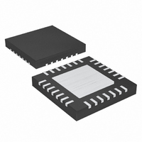
MAX9729ETI+T Maxim Integrated Products, MAX9729ETI+T Datasheet - Page 9

MAX9729ETI+T
Manufacturer Part Number
MAX9729ETI+T
Description
IC AMP AUDIO .052W STER 28TQFN
Manufacturer
Maxim Integrated Products
Series
DirectDrive™r
Type
Class ABr
Datasheet
1.MAX9729ETI.pdf
(28 pages)
Specifications of MAX9729ETI+T
Output Type
Headphones, 2-Channel (Stereo)
Max Output Power X Channels @ Load
52mW x 2 @ 32 Ohm
Voltage - Supply
1.8 V ~ 3.6 V
Features
Bass Boost, Depop, I²C, Input Multiplexer, Short-Circuit and Thermal Protection, Shutdown, Volume Control
Mounting Type
Surface Mount
Package / Case
28-TQFN Exposed Pad
Lead Free Status / RoHS Status
Lead free / RoHS Compliant
(V
BM_ = 0V, maximum gain setting = 3.5dB, volume attenuation setting = 0dB (total voltage gain = 3.5dB), BassMax disabled. Load
connected between OUT_ and PGND where specified. THD+N measurement BW = 22Hz to 22kHz. Both channels loaded and driven
in phase. T
200mV/div
200mV/div
100mV/div
DD
4, 8, 15,
PIN
22
10
11
12
13
14
= PV
1
2
3
5
6
7
9
DD
A
Stereo Headphone Amplifier with BassMax,
= +25°C, unless otherwise noted.)
= SHDN = 3V, PGND = SGND = 0V, C1 = C2 = C3 = 1µF, C
NAME
SGND
PGND
PV
PV
SV
INR2
INR3
FADER OPERATION
N.C.
ADD
SDA
C1N
C1P
SCL
DD
SS
SS
_______________________________________________________________________________________
20ms/div
Right-Channel Input 2
Right-Channel Input 3
Signal Ground. Connect SGND to PGND at a single point on the PCB near the device.
No Connection. Not internally connected.
Slave Address Selection Input. Connect ADD to V
PGND to set the device slave address to 1010000.
Charge-Pump Output. Connect to SV
Serial Data Input. Connect a pullup resistor greater than 500Ω from SDA to PV
Charge-Pump Flying Capacitor Negative Terminal. Connect a 1µF capacitor between C1P and C1N.
Power Ground. Connect PGND to SGND at a single point on the PCB near the device.
Charge-Pump Flying Capacitor Positive Terminal. Connect a 1µF capacitor between C1P and C1N.
Serial Clock Input. Connect a pullup resistor greater than 500Ω from SCL to PV
Charge-Pump and Logic Power-Supply Input. Bypass PV
to V
as close to the device as possible.
Headphone Amplifier Negative Power-Supply Input. Connect to PV
to PGND.
DD
. PV
MAX9729 toc28
DD
and V
DD
Volume Control, and Input Mux
Typical Operating Characteristics (continued)
are internally connected and should each have a 1µF bypass capacitor located
6
5
4
3
2
1.8
NO LOAD
INPUTS AC-GROUNDED
2.0
2.2
vs. SUPPLY VOLTAGE
SUPPLY CURRENT
SUPPLY VOLTAGE (V)
2.4
SS
.
2.6
2.8
FUNCTION
IN
3.0
= 1µF (1206 case size, X7R dielectric ceramic capacitor),
DD
3.2
to set the device slave address to 1010001 or to
3.4
DD
3.6
to PGND with a 1µF capacitor and connect
SS
7
6
5
4
3
2
1
0
and bypass with a 1µF capacitor
1.8
2.0
DD
2.2
DD
Pin Description
SHUTDOWN CURRENT
vs. SUPPLY VOLTAGE
.
SUPPLY VOLTAGE (V)
.
2.4
2.6
2.8
3.0
3.2
3.4
3.6
9


